1. The delay problem
Under the same core frequency, the actual operating frequency of DDR2 is twice that of DDR. This is due to the fact that DDR2 memory has twice the 4BIT pre-read capability of standard DDR memory. In other words, although DDR2, like DDR, uses the basic method of data transmission at the same time as the clock rise delay and fall delay, DDR2 has twice the ability of DDR to pre-read system command data. In other words, under the same operating frequency of 100MHz, the actual frequency of DDR is 200MHz, while DDR2 can reach 400MHz.
In this way, another problem arises: in DDR and DDR2 memory with the same operating frequency, the memory latency of the latter is slower than the former. For example, DDR 200 and DDR2-400 have the same delay, while the latter has twice the bandwidth. In fact, DDR2-400 and DDR 400 have the same bandwidth, they are both 3.2GB/s, but the core operating frequency of DDR400 is 200MHz, and the core operating frequency of DDR2-400 is 100MHz, which means the delay of DDR2-400 It is higher than DDR400.
2. Packaging and heat generation
The biggest breakthrough of DDR2 memory technology is actually not that users think twice the transmission capacity of DDR, but with lower heat generation and lower power consumption, DDR2 can achieve faster frequency increases and breakthroughs. The 400MHZ limit of standard DDR.
DDR memory is usually packaged in TSOP chip. This package can work well at 200MHz. When the frequency is higher, its long pins will generate high impedance and parasitic capacitance, which will affect its performance. The difficulty of stability and frequency improvement. This is why it is difficult for the core frequency of DDR to break through 275MHZ. And DDR2 memory adopts FBGA package form. Different from the currently widely used TSOP package, the FBGA package provides better electrical performance and heat dissipation, which provides a good guarantee for the stable operation of DDR2 memory and the development of future frequencies.
DDR2 memory uses 1.8V voltage, which is much lower than the DDR standard 2.5V, thus providing significantly smaller power consumption and less heat. This change is significant.
In addition to the differences mentioned above, DDR2 also introduces three new technologies, they are OCD, ODT and Post CAS.
① OCD (Off-Chip Driver): This is the so-called offline driver adjustment. DDR II can improve signal integrity through OCD. DDR II adjusts the pull-up/pull-down resistance value to make the two voltages equal. Use OCD to improve signal integrity by reducing the tilt of DQ-DQS; improve signal quality by controlling voltage.
② ODT: ODT is the termination resistor of the built-in core. We know that a large number of termination resistors are required on the motherboard using DDR SDRAM in order to prevent the data line terminal from reflecting signals. It greatly increases the manufacturing cost of the motherboard. In fact, different memory modules have different requirements for the termination circuit. The size of the termination resistor determines the signal ratio and reflectivity of the data line. If the termination resistance is small, the data line signal reflection is low but the signal-to-noise ratio is also low; If the termination resistance is high, the signal-to-noise ratio of the data line will be high, but the signal reflection will also increase. Therefore, the termination resistance on the motherboard cannot match the memory module very well, and it will affect the signal quality to a certain extent. DDR2 can build in suitable termination resistors according to its own characteristics, so as to ensure the best signal waveform. Using DDR2 can not only reduce the cost of the motherboard, but also get the best signal quality, which is unmatched by DDR.
③ Post CAS: It is set to improve the utilization efficiency of DDR II memory. In Post CAS operation, the CAS signal (read/write/command) can be inserted one clock cycle after the RAS signal, and the CAS command can remain valid after the additional delay (Additive Latency). The original tRCD (RAS to CAS and delay) is replaced by AL (Additive Latency), which can be set in 0, 1, 2, 3, 4. Since the CAS signal is placed one clock cycle after the RAS signal, the ACT and CAS signals will never collide.
In general, DDR2 uses many new technologies to improve many of DDR's shortcomings. Although it currently has many shortcomings in terms of high cost and slow latency, it is believed that with the continuous improvement and improvement of technology, these problems will eventually be resolved.
(1) DDR2 technical specifications
The starting frequency of DDR2 memory will start from 400Mhz, the highest standard frequency of DDR memory. The frequencies that can be produced are now defined to support 533Mhz to 667Mhz. The standard operating frequency is 200/266/333MHz, and the operating voltage is 1.8V. DDR2 uses the newly defined 240 PIN DIMM interface standard, which is completely incompatible with the existing DDR 184PIN DIMM interface standard. This means that all existing motherboards with DDR standard interfaces cannot use DDR2 memory. This will become a major obstacle to the popularization of DDR2 memory standards. Fortunately, INTEL's next-generation platform will fully support the 240PIN DDR2 interface, laying the foundation for the popularization of DDR2 in 2005.
I believe everyone has already seen that a variety of graphics card products using DDR2 memory have been launched on the market. However, the production standards and methods of DDR2 memory used on graphics cards are completely different from the DDR2 technology used on desktop system applications. This article will not make a detailed distinction for the time being, but everyone should be clear about why a large number of applications are already available on graphics cards but desktop systems are not.
Compared with the previous generation of standard DDR technology, DDR2 memory technology uses a simple and clear way. Although DDR2, like DDR, uses the basic method of data transmission at the same time as the clock rise delay and fall delay, the biggest difference is that DDR2 The memory can perform 4bit pre-reading. Twice the 2BIT pre-reading of standard DDR memory, which means that DDR2 has twice the capacity of pre-reading system command data. I have understood what I think, for this reason, DDR2 simply obtains the complete data transmission capacity twice that of DDR. So the author tells you that DDR2 400Mhz is also named PC3200, please keep reading, why?
The biggest breakthrough point of DDR2 memory technology is not actually the transmission capacity that the judges think is twice that of DDR, but rather, it achieves a faster frequency increase with lower heat generation and lower power consumption. Break through the 400MHZ limit of standard DDR. It seems that this seems more magical, breaking the maximum frequency limit, and even reducing heat generation and power consumption? Although DDR2 technology also uses several new technologies to complete the above capabilities, the key lies in the pre-reading capability of 4BIT. The author will take you step by step.
(2) DDR2 frequency and bandwidth
In addition to the frequency and bandwidth of the three DDR2 memory standards that have been released, it is worth noting that DDR2 400Mhz and DDR400Mhz have the same bandwidth of 3.2GB. Also, with the aid of dual-channel memory technology, 667MHZ DDR2 will Provides an amazing bandwidth of up to 10.6GB/S!
The initial capacity of DDR2 memory is 256MB, up to 512MB, 1G. Provides sufficient capacity guarantee on the desktop system. Theoretically, the high-density features of DDR2 memory particles can support a maximum capacity of 4G and above, which is widely used in professional fields. It may even bring nGB-level super capacity to PC systems in the next few years.
The DDR2 standard stipulates that all DDR2 memories are packaged in FBGA. Different from the widely used TSOP and TSOP-II packages, the FBGA package provides better electrical performance and heat dissipation, which provides a good guarantee for the stable operation of DDR2 memory and the development of future frequencies. At present, all the DDR2 memory particles on the graphics card are used in the FBGA package mode. DDR2 memory uses 1.8V voltage, which is much lower than the DDR standard 2.5V, thus providing significantly smaller power consumption and less heat. This change is significant, and it also allows DDR2 The memory is more suitable for notebooks and laptops. Since it can work at such a low voltage, how can the frequency increase be achieved?
(3) DDR2 working principle
As everyone knows, the basic working steps of memory are divided into: pre-reading data from the system → saving in the memory unit queue → transferring to the memory I/O buffer → transferring to the CPU system for processing.
DDR memory uses a core frequency of 200MHZ, which is synchronously transmitted to the I/O cache through two routes, and it is the actual frequency to achieve 400MHZ.
DDR2 uses a core frequency of 100MHZ, which is synchronously transmitted to the I/O buffer through four transmission routes, and also achieves an actual frequency of 400MHZ.
The clever magistrate has already seen the mystery. It is precisely because DDR2 can pre-read 4BIT data, it can use four-way transmission, and because DDR can only pre-read 2BIT data, it can only use two 200MHZ transmission lines to achieve 400MHZ. In this way, DDR2 can completely reduce the core frequency to 100MHZ without reducing the total frequency, so that it can easily achieve smaller heat dissipation and lower voltage requirements. Moreover, the core frequency can be further increased to achieve 133*4, 166*4, and a maximum of 200*4 to reach 800MHZ. However, everyone knows that lower memory latency can bring higher performance. Then, in DDR2, in order to ensure the stability and smoothness of 4-channel transmission and avoid electrical interference and data conflicts, a slightly larger memory than DDR is used. Delay setting. I believe smart judges can also see that this is actually a far-sighted design.
(4) New feature technology of DDR2
After understanding the technical principles of DDR II, let's take a look at the three main new features of DDR II: They are OCD, ODT and Post CAS.
OCD (Off-Chip Driver), also known as offline drive adjustment, DDR II can improve signal integrity through OCD. DDR II adjusts the pull-up/pull-down resistance value to make the two voltages equal. That is, Pull-up=Pull-down. Use OCD to improve signal integrity by reducing the tilt of DQ-DQS; improve signal quality by controlling voltage.
ODT is a termination resistor for the built-in core. We know that a large number of termination resistors are required on motherboards using DDR I SDRAM, at least one termination resistor is required for each data line, which is not a small cost for the motherboard. The use of termination resistors on the signal line is to prevent the data line terminal from reflecting signals, so a termination resistor with a certain resistance is required. This resistance is too large or too small. The signal-to-noise ratio of the circuit with a larger resistance is higher but the signal reflection is more serious. A small resistance can reduce the signal reflection but will cause the signal-to-noise ratio to drop. In addition, since different memory modules may not have exactly the same termination resistance requirements, the motherboard is also more picky about memory modules.
DDR II has a built-in termination resistor, which turns off the termination resistor when the DRAM particles are working, and turns on the termination resistor for non-working DRAM particles to reduce signal reflection. ODT brings at least two benefits to DDR II. One is that the elimination of the termination resistor on the motherboard reduces the cost of the motherboard and makes the design of the PCB board easier. The second advantage is that the termination resistor can match the "characteristics" of the memory particles, so that the DRAM is in the best condition.
Post CAS, it is set to improve the utilization efficiency of DDR II memory. In Post CAS operation, the CAS signal (read/write/command) can be inserted one clock cycle after the RAS signal, and the CAS command can remain valid after the additional delay (Additive Latency). The original tRCD (RAS to CAS and delay) is replaced by AL (Additive Latency), which can be set in 0, 1, 2, 3, 4. Since the CAS signal is placed one clock cycle after the RAS signal, the ACT and CAS signals will never collide.
In normal operation, the various memory parameters at this time are: tRRD=2, tRCD=4, CL=4, AL=0, BL=4 (BL is the burst data length, Burst Length). We see that tRRD (the delay from RAS to RAS) is two clock cycles, and tRCD (the delay from RAS to CAS) is four clock cycles, so the ACT (segment activation) and CAS signals collide on the fourth clock cycle. , ACT moves backward by one clock cycle, so you can see that there is a clock cycle of BUBBLE in the middle of the subsequent data transmission.
Let's take a look at the operation of Post CAS. The memory parameters at this time are: tRRD=2, tRCD=4, CL=4, AL=3, BL=4. RAS is set in a clock cycle after the ACT signal, so CAS and ACT will not conflict, tRCD is replaced by AL (in fact, you can imagine that tRCD has not been reduced, but is a conceptual change, CAS goes backwards One clock cycle, but AL is shorter than tRCD, the collision of the signal command can be cancelled by adjusting), and the DRAM keeps the read command during the additional delay. Due to this design, ACT and CAS will no longer collide, and there will be no BUBBLE in the memory read timing.
Using Post CAS plus Additive Latency will bring three benefits:
1. The Collision phenomenon on the command bus can be easily cancelled
2. Improve the efficiency of the command and data bus
3. Without Bubble, the actual memory bandwidth can be improved
Another ordinary DOTHAN FSB is 533, which means that the memory with DDR533 can just meet the memory bandwidth, but the current notebook DDR1 only has DDR400 at most, and generally 333 cannot meet the FSB of DOTHAN. At this time, the memory becomes the bottleneck of the system. After the 915 platform comes out It can support DDR2 dual-channel DDR2 starting from 400 and up to 533.
At this time, you may have discovered that in fact, single-channel DDR2 533 can fully meet DOTHAN's FSB, that is to say, DDR2 533 has dual-channel, only FSB=1066 CPU can match it. Before INTEL1066FSB U came out, DDR2 533 dual-channel is basically Waste, so the performance improvement that DDR2 dual-channel brings to the Sonama platform is very small. DOTHAN has become the bottleneck of the Sonama system. Friends who are not demanding on performance do not need to spend money on dual-channel DDR2.


|
|
|
|
How far(long) the transmitter cover?
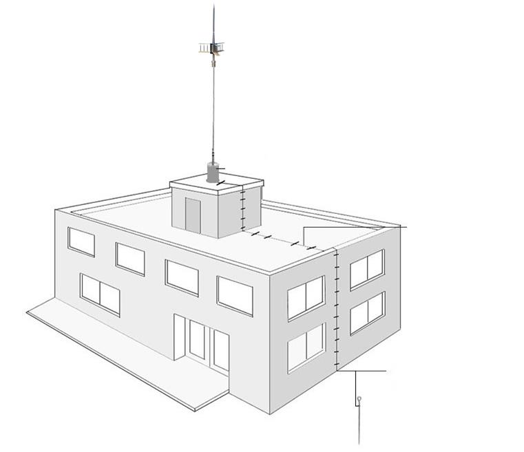
The transmission range depends on many factors. The true distance is based on the antenna installing height , antenna gain, using environment like building and other obstructions , sensitivity of the receiver, antenna of the receiver . Installing antenna more high and using in the countryside , the distance will much more far.
EXAMPLE 5W FM Transmitter use in the city and hometown:
I have a USA customer use 5W fm transmitter with GP antenna in his hometown ,and he test it with a car, it cover 10km(6.21mile).
I test the 5W fm transmitter with GP antenna in my hometown ,it cover about 2km(1.24mile).
I test the 5W fm transmitter with GP antenna in Guangzhou city ,it cover about only 300meter(984ft).
Below are the approximate range of different power FM Transmitters. ( The range is diameter )
0.1W ~ 5W FM Transmitter :100M ~1KM
5W ~15W FM Ttransmitter : 1KM ~ 3KM
15W ~ 80W FM Transmitter : 3KM ~10KM
80W ~500W FM Transmitter : 10KM ~30KM
500W ~1000W FM Transmitter : 30KM ~ 50KM
1KW ~ 2KW FM Transmitter : 50KM ~100KM
2KW ~5KW FM Transmitter : 100KM ~150KM
5KW ~10KW FM Transmitter : 150KM ~200KM
How to contact us for the transmitter?
Call me +8618078869184 OR
whatsapp:+86 18319244009
Email me [email protected]
1.How far you want to cover in diameter ?
2.How tall of you tower ?
3.Where are you from ?
And we will give you more professional advice.
About Us
FMUSER.ORG is a system integration company focusing on RF wireless transmission / studio video audio equipment / streaming and data processing .We are providing everything from advice and consultancy through rack integration to installation, commissioning and training.
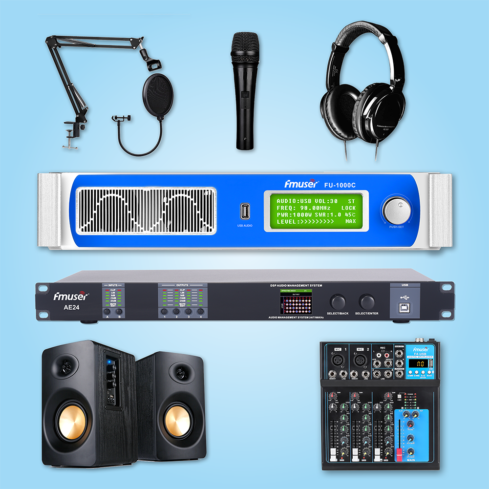
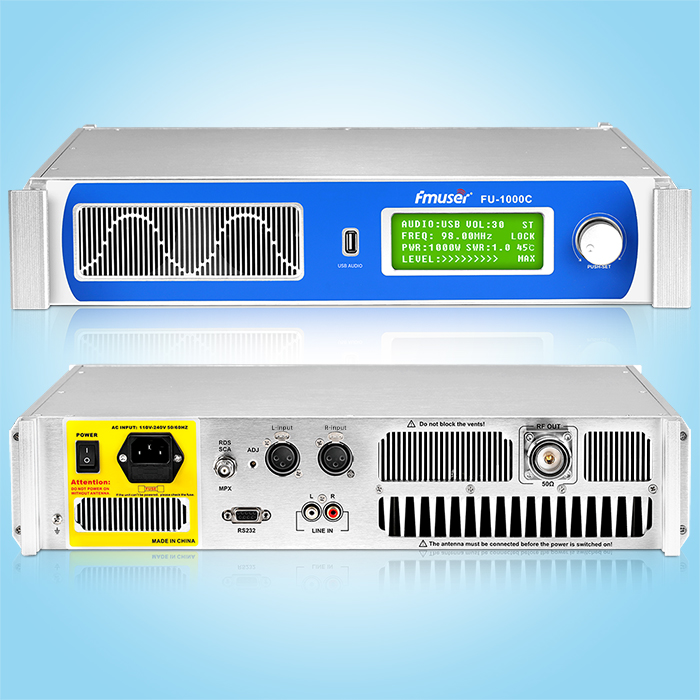
We offer FM Transmitter, Analog TV Transmitter, Digital TV transmitter, VHF UHF Transmitter, Antennas, Coaxial Cable Connectors, STL, On Air Processing, Broadcast Products for the Studio, RF Signal Monitoring, RDS Encoders, Audio Processors and Remote Site Control Units, IPTV Products, Video / Audio Encoder / Decoder, designed to meet the needs of both large international broadcast networks and small private stations alike.
Our solution has FM Radio Station / Analog TV Station / Digital TV Station / Audio Video Studio Equipment / Studio Transmitter Link / Transmitter Telemetry System / Hotel TV System / IPTV Live Broadcasting / Streaming Live Broadcast / Video Conference / CATV Broadcasting system.
We are using advanced technology products for all the systems, because we know the high reliability and high performance are so important for the system and solution . At the same time we also have to make sure our products system with a very reasonable price.
We have customers of public and commercial broadcasters, telecom operators and regulation authorities , and we also offer solution and products to many hundreds of smaller, local and community broadcasters .
FMUSER.ORG has been exporting more than 15 years and have clients all over the world. With 13 years experience in this field ,we have a professional team to solve customer's all kinds of problems. We dedicated in supplying the extremely reasonable pricing of professional products & services. Contact email : [email protected]
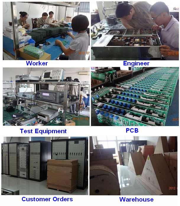
Our Factory

We have modernization of the factory . You are welcome to visit our factory when you come to China.

At present , there are already 1095 customers around the world visited our Guangzhou Tianhe office . If you come to China , you are welcome to visit us .
At Fair

This is our participation in 2012 Global Sources Hong Kong Electronics Fair . Customers from all over the world finally have a chance to get together.
Where is Fmuser ?

You can search this numbers " 23.127460034623816,113.33224654197693 " in google map , then you can find our fmuser office .
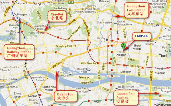
FMUSER Guangzhou office is in Tianhe District which is the center of the Canton . Very near to the Canton Fair , guangzhou railway station, xiaobei road and dashatou , only need 10 minutes if take TAXI . Welcome friends around the world to visit and negotiate .
Contact: Kerwin
Cellphone: +8618078869184
whatsapp:+86 18319244009
Wechat: +8618078869184
E-mail: [email protected]
Address: No.305 Room HuiLan Building No.273 Huanpu Road Guangzhou China Zip:510620
|
|
|
|
English: We accept all payments , such as PayPal, Credit Card, Western Union, Alipay, Money Bookers, T/T, LC, DP, DA, OA, Payoneer, If you have any question , please contact me [email protected] or
whatsapp:+86 18319244009
-
PayPal.  www.paypal.com www.paypal.com
We recommend you use Paypal to buy our items ,The Paypal is a secure way to buy on internet .
Every of our item list page bottom on top have a paypal logo to pay.
Credit Card.If you do not have paypal,but you have credit card,you also can click the Yellow PayPal button to pay with your credit card.
---------------------------------------------------------------------
But if you have not a credit card and not have a paypal account or difficult to got a paypal accout ,You can use the following:
Western Union.  www.westernunion.com www.westernunion.com
Pay by Western Union to me :
First name/Given name: Yingfeng
Last name/Surname/ Family name: Zhang
Full name: Yingfeng Zhang
Country: China
City: Guangzhou
|
---------------------------------------------------------------------
T/T . Pay by T/T (wire transfer/ Telegraphic Transfer/ Bank Transfer)
First BANK INFORMATION (COMPANY ACCOUNT):
SWIFT BIC: BKCHHKHHXXX
Bank name: BANK OF CHINA (HONG KONG) LIMITED, HONG KONG
Bank Address: BANK OF CHINA TOWER, 1 GARDEN ROAD, CENTRAL, HONG KONG
BANK CODE: 012
Account Name : FMUSER INTERNATIONAL GROUP LIMITED
Account NO. : 012-676-2-007855-0
---------------------------------------------------------------------
Second BANK INFORMATION (COMPANY ACCOUNT):
Beneficiary: Fmuser International Group Inc
Account Number: 44050158090900000337
Beneficiary's Bank: China Construction Bank Guangdong Branch
SWIFT Code: PCBCCNBJGDX
Address: NO.553 Tianhe Road, Guangzhou, Guangdong,Tianhe District, China
**Note: When you transfer money to our bank account, please DO NOT write anything in the remark area, otherwise we won't be able to receive the payment due to government policy on international trade business.
|
|
|
|
* It will be sent in 1-2 working days when payment clear.
* We will send it to your paypal address. If you want to change address, please send your correct address and phone number to my email [email protected]
* If the packages is below 2kg,we will be shipped via post airmail, it will take about 15-25days to your hand.
If the package is more than 2kg,we will ship via EMS , DHL , UPS, Fedex fast express delivery,it will take about 7~15days to your hand.
If the package more than 100kg , we will send via DHL or air freight. It will take about 3~7days to your hand.
All the packages are form China guangzhou.
* Package will be sent as a "gift" and declear as less as possible,buyer don't need to pay for "TAX".
* After ship, we will send you an E-mail and give you the tracking number.
|
|
|
For Warranty .
Contact US--->>Return the item to us--->>Receive and send another replace .
Please return to this address and write your paypal address,name,problem on note: |
|


