Field effect transistors are different from bipolar transistors in that they operate only with one of electrons or holes. According to the structure and principle, it can be divided into:
. Junction field effect tube
. MOS type field effect tube
1. Junction FET (junction FET)
1) Principle
As shown in the figure, the N-channel junction field effect transistor has a structure in which the N-type semiconductor is clamped from both sides by the gate of the P-type semiconductor. The depletion area generated when a reverse voltage is applied to the PN junction is used for current control.
When a DC voltage is applied to both ends of the N-type crystal region, electrons flow from the source to the drain. The width of the channel through which electrons pass is determined by the P-type region diffused from both sides and the negative voltage applied to this region.
When the negative gate voltage is strengthened, the depletion area of the PN junction extends into the channel, and the channel width is reduced. Therefore, the source-drain current can be controlled by the voltage of the gate electrode.
2) Use
Even if the gate voltage is zero, there is current flow, so it is used for constant current sources or for audio amplifiers due to low noise.
2. MOS type field effect tube
1) Principle
Even in the structure (MOS structure) of the metal (M) and the semiconductor (S) sandwiching the oxide film (O), if a voltage is applied between the (M) and the semiconductor (S), a depletion layer can be generated. In addition, when a higher voltage is applied, electrons or holes can be accumulated under the oxygen bloom film to form an inversion layer. The MOSFET is used as a switch.
In the operation principle diagram, if the gate voltage is zero, the PN junction will disconnect the current, so that the current does not flow between the source and the drain. If a positive voltage is applied to the gate, the holes of the P-type semiconductor will be expelled from the oxide film-the surface of the P-type semiconductor under the gate to form a depletion layer. Moreover, if the gate voltage is increased again, electrons will be attracted to the surface to form a thinner N-type inversion layer, so that the source pin (N-type) and the drain (N-type) are connected, allowing current to flow .
2) Use
Because of its simple structure, fast speed, simple gate drive, strong destructive power and other characteristics, and the use of microfabrication technology, it can directly improve performance, so it is widely used in high-frequency devices from LSI basic devices to Power devices (power control devices) and other fields.
3. Common field utility tube
1) MOS field effect tube
That is, the metal-oxide-semiconductor field effect tube, the English abbreviation is MOSFET (Metal-Oxide-Semiconductor
Field-Effect-Transistor), which is an insulated gate type. Its main feature is that there is a silicon dioxide insulating layer between the metal gate and the channel, so it has a very high input resistance (most High up to 1015Ω). It is also divided into N-channel tube and P-channel tube, the symbol is shown in Figure 1. Usually the substrate (substrate) and the source S are connected together. According to the different conduction mode, MOSFET is divided into enhancement type,
Depletion type. The so-called enhanced type refers to: when VGS=0, the tube is in an off state, and after adding the correct VGS, the majority of carriers are attracted to the gate, thereby "enhancing" the carriers in this area and forming a conductive channel .
The depletion type means that when VGS=0, a channel is formed, and when the correct VGS is added, the majority of carriers can flow out of the channel, thus "depleting" the carriers and turning the tube off.
Taking the N channel as an example, it is made on a P-type silicon substrate with two source diffusion regions N+ and drain diffusion regions N+ with a high doping concentration, and then the source S and the drain D are led out respectively. The source electrode and the substrate are connected internally, and the two always keep the same electric
Bit. The front direction in the symbol of Figure 1(a) is from the outside to the electricity, which means from the P-type material (substrate) to the N-type channel. When the drain is connected to the positive pole of the power supply, the source is connected to the negative pole of the power supply and VGS=0, the channel current (that is, the drain current
Stream) ID=0. With the gradual increase of VGS, attracted by the positive voltage of the gate, negatively charged minority carriers are induced between the two diffusion regions, forming an N-type channel from the drain to the source. When VGS is greater than the tube of When the turn-on voltage VTN (generally about +2V), the N-channel tube begins to conduct, forming a drain current ID.
MOS field effect tube is more "squeaky". This is because its input resistance is very high, and the capacitance between the gate and the source is very small, and it is very susceptible to being charged by the external electromagnetic field or electrostatic induction, and a small amount of charge can be formed on the capacitance between the electrodes.
To a very high voltage (U=Q/C), the tube will be damaged. Therefore, the pins are twisted together at the factory, or installed in metal foil, so that the G pole and the S pole are at the same potential to prevent the accumulation of static charge. When the tube is not in use, use all The wires should also be shorted. Be extra careful when measuring, and take corresponding anti-static measures.
2) Detection method of MOS field effect tube
(1). Preparations Before measuring, short-circuit the human body to ground before touching the pins of the MOSFET. It is best to connect a wire to the wrist to connect with the earth, so that the human body and the earth maintain an equipotential. Separate the pins again, and then remove the wires.
(2). Determination electrode
Set the multimeter to the R×100 gear, and first determine the grid. If the resistance of a pin and other pins are both infinite, it proves that this pin is the grid G. Exchange the test leads to re-measure, the resistance value between S-D should be several hundred ohms to several thousand
Oh, where the resistance value is smaller, the black test lead is connected to the D pole, and the red test lead is connected to the S pole. For the 3SK series products produced in Japan, the S pole is connected to the shell, so it is easy to determine the S pole.
(3). Check amplification capability (transconductance)
Hang the G pole in the air, connect the black test lead to the D pole, and the red test lead to the S pole, and then touch the G pole with your finger, the needle should have a larger deflection. The double-gate MOS field effect transistor has two gates G1 and G2. To distinguish it, you can touch it with your hands
G1 and G2 poles, the G2 pole is the one with the larger deflection of the watch hand to the left. At present, some MOSFET tubes have added protective diodes between the G-S poles, and there is no need to short-circuit each pin.
3) Precautions for the use of MOS field effect transistors.
MOS field effect transistors should be classified when they are used and cannot be interchanged at will. MOS field effect transistors are easily broken down by static electricity due to their high input impedance (including MOS integrated circuits). Pay attention to the following rules when using them:
MOS devices are usually packed in black conductive foam plastic bags when they leave the factory. Do not pack them in a plastic bag by yourself. You can also use thin copper wires to connect the pins together, or wrap them in tin foil
The MOS device taken out cannot slide on the plastic board, and a metal plate is used to hold the device to be used.
The soldering iron must be well grounded.
Before welding, the power line of the circuit board should be short-circuited with the ground line, and then the MOS device should be separated after the welding is completed.
The welding sequence of each pin of the MOS device is drain, source, and gate. When disassembling the machine, the sequence is reversed.
Before installing the circuit board, use a grounded wire clamp to touch the terminals of the machine, and then connect the circuit board.
The gate of the MOS field effect transistor is preferably connected to a protection diode when allowed. When overhauling the circuit, pay attention to check whether the original protection diode is damaged.
4) VMOS field effect tube
VMOS field effect tube (VMOSFET) is abbreviated as VMOS tube or power field effect tube, and its full name is V-groove MOS field effect tube. It is a newly developed high-efficiency, power switch after MOSFET
Pieces. It not only inherits the high input impedance of the MOS field effect tube (≥108W), small drive current (about 0.1μA), but also has high withstand voltage (up to 1200V) and large working current
(1.5A~100A), high output power (1~250W), good transconductance linearity, fast switching speed and other excellent characteristics. It is precisely because it combines the advantages of electron tubes and power transistors into one, so the voltage
Amplifiers (voltage amplification up to several thousand times), power amplifiers, switching power supplies and inverters are being widely used.
As we all know, the gate, source, and drain of a traditional MOS field effect transistor are on a chip where the gate, source, and drain are roughly on the same horizontal plane, and its working current basically flows in a horizontal direction. VMOS tube is different, from the bottom left picture you can
Two major structural characteristics can be seen: first, the metal gate adopts a V-groove structure; second, it has vertical conductivity. Since the drain is drawn from the back of the chip, the ID does not flow horizontally along the chip, but is heavily doped with N+
Starting from the region (source S), it flows into the lightly doped N-drift region through the P channel, and finally reaches the drain D vertically downwards. The direction of the current is shown by the arrow in the figure, because the cross-sectional area of the flow is increased, so large current can pass. Because in the gate
There is a silicon dioxide insulating layer between the pole and the chip, so it is still an insulated gate MOS field effect transistor.
The main domestic manufacturers of VMOS field effect transistors include 877 Factory, Tianjin Semiconductor Device Fourth Factory, Hangzhou Electron Tube Factory, etc. Typical products include VN401, VN672, VMPT2, etc.
5) Detection method of VMOS field effect tube
(1). Determine the grid G. Set the multimeter to the R×1k position to measure the resistance between the three pins. If it is found that the resistance of a pin and its two pins are both infinite, and it is still infinite after exchanging the test leads, it is proved that this pin is the G pole, because it is insulated from the other two pins.
(2). Determining the source S and drain D As can be seen from Figure 1, there is a PN junction between the source and the drain. Therefore, according to the difference in the forward and reverse resistance of the PN junction, the S pole and the D pole can be identified. Use the exchange meter pen method to measure the resistance twice, and the one with the lower resistance value (generally several thousand ohms to ten thousand ohms) is the forward resistance. At this time, the black test lead is S pole, and the red one is connected to D pole.
(3). Measure the drain-source on-state resistance RDS(on) to short-circuit the G-S pole. Choose the R×1 gear of the multimeter. Connect the black test lead to the S pole and the red test lead to the D pole. The resistance should be a few ohms to more than ten ohms.
Due to different test conditions, the measured RDS(on) value is higher than the typical value given in the manual. For example, an IRFPC50 VMOS tube is measured with a 500-type multimeter R×1 file, RDS
(On)=3.2W, greater than 0.58W (typical value).
(4). Check the transconductance. Place the multimeter in the R×1k (or R×100) position. Connect the red test lead to the S pole, and the black test lead to the D pole. Hold a screwdriver to touch the grid. The needle should deflect significantly. The greater the deflection, the greater the deflection of the tube. The higher the transconductance.
6) Matters needing attention:
VMOS tubes are also divided into N-channel tubes and P-channel tubes, but most of the products are N-channel tubes. For P-channel tubes, the position of the test leads should be exchanged during measurement.
There are a few VMOS tubes with protection diodes between G-S, items 1 and 2 in this detection method are no longer applicable.
At present, there is also a VMOS tube power module on the market, which is specially used for AC motor speed controllers and inverters. For example, the IRFT001 module produced by the American IR company has three N-channel and P-channel tubes inside, forming a three-phase bridge structure.
The VNF series (N-channel) products on the market are ultra-high frequency power field effect transistors produced by Supertex in the United States. Its highest operating frequency is fp=120MHz, IDSM=1A, PDM=30W, common source small signal low-frequency transconductance gm =2000μS. It is suitable for high-speed switching circuits and broadcasting and communication equipment.
When using a VMOS tube, a suitable heat sink must be added. Taking VNF306 as an example, the maximum power can reach 30W after installing a 140×140×4 (mm) radiator.
7) Comparison of field effect tube and transistor
The field effect tube is the voltage control element, and the transistor is the current control element. When only allowing less current to be drawn from the signal source, a FET should be used; and when the signal voltage is low and allowing more current to be drawn from the signal source, a transistor should be used.
The field effect transistor uses majority carriers to conduct electricity, so it is called a unipolar device, while the transistor has both majority carriers and minority carriers to conduct electricity. It is called a bipolar device.
The source and drain of some field effect transistors can be used interchangeably, and the gate voltage can also be positive or negative, which is more flexible than transistors.
The field effect tube can work under very small current and very low voltage, and its manufacturing process can easily integrate many field effect tubes on a silicon chip, so the field effect tube has been used in large-scale integrated circuits. Wide range of applications.


|
|
|
|
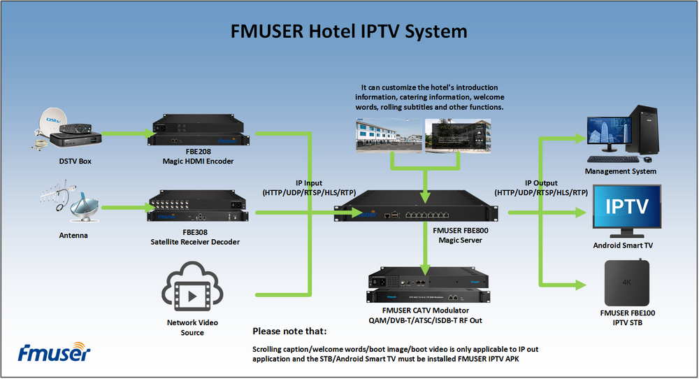
How far(long) the transmitter cover?
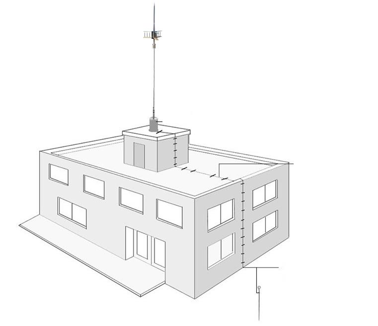
The transmission range depends on many factors. The true distance is based on the antenna installing height , antenna gain, using environment like building and other obstructions , sensitivity of the receiver, antenna of the receiver . Installing antenna more high and using in the countryside , the distance will much more far.
EXAMPLE 5W FM Transmitter use in the city and hometown:
I have a USA customer use 5W fm transmitter with GP antenna in his hometown ,and he test it with a car, it cover 10km(6.21mile).
I test the 5W fm transmitter with GP antenna in my hometown ,it cover about 2km(1.24mile).
I test the 5W fm transmitter with GP antenna in Guangzhou city ,it cover about only 300meter(984ft).
Below are the approximate range of different power FM Transmitters. ( The range is diameter )
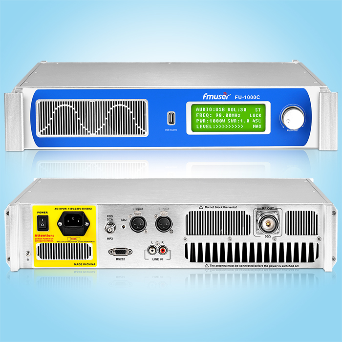
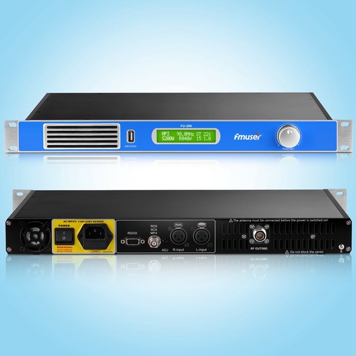
0.1W ~ 5W FM Transmitter :100M ~1KM
5W ~15W FM Ttransmitter : 1KM ~ 3KM
15W ~ 80W FM Transmitter : 3KM ~10KM
80W ~500W FM Transmitter : 10KM ~30KM
500W ~1000W FM Transmitter : 30KM ~ 50KM
1KW ~ 2KW FM Transmitter : 50KM ~100KM
2KW ~5KW FM Transmitter : 100KM ~150KM
5KW ~10KW FM Transmitter : 150KM ~200KM
How to contact us for the transmitter?
Call me +8618078869184 OR
Email me [email protected]
1.How far you want to cover in diameter ?
2.How tall of you tower ?
3.Where are you from ?
And we will give you more professional advice.
About Us
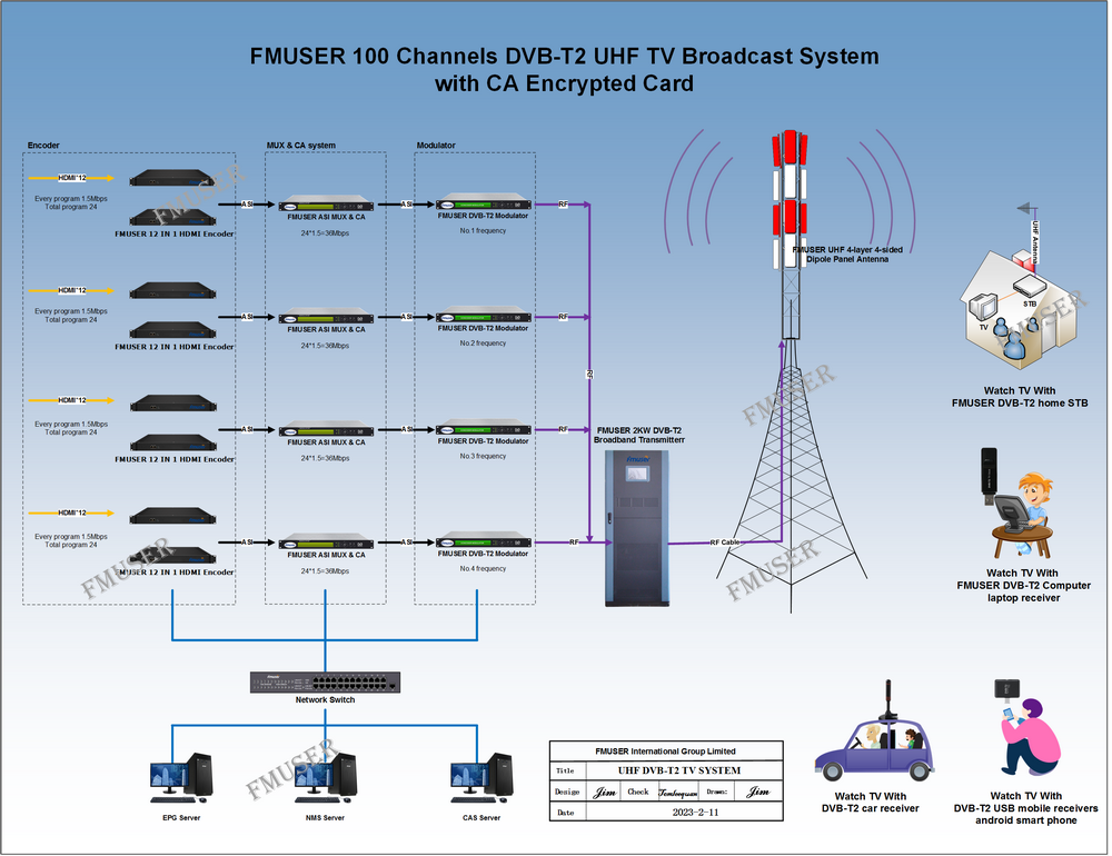
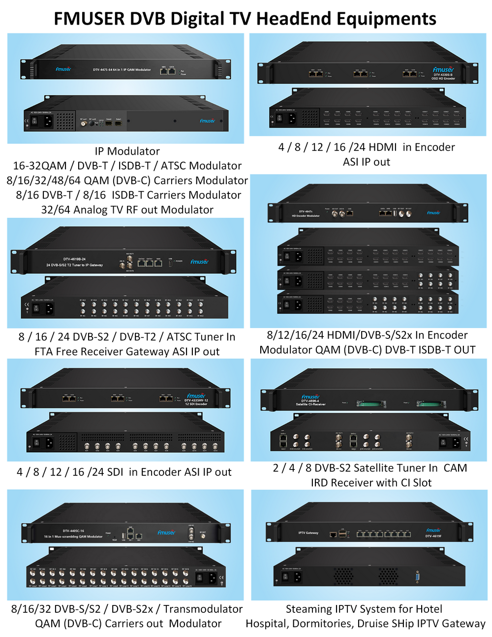
FMUSER.ORG is a system integration company focusing on RF wireless transmission / studio video audio equipment / streaming and data processing .We are providing everything from advice and consultancy through rack integration to installation, commissioning and training.
We offer FM Transmitter, Analog TV Transmitter, Digital TV transmitter, VHF UHF Transmitter, Antennas, Coaxial Cable Connectors, STL, On Air Processing, Broadcast Products for the Studio, RF Signal Monitoring, RDS Encoders, Audio Processors and Remote Site Control Units, IPTV Products, Video / Audio Encoder / Decoder, designed to meet the needs of both large international broadcast networks and small private stations alike.
Our solution has FM Radio Station / Analog TV Station / Digital TV Station / Audio Video Studio Equipment / Studio Transmitter Link / Transmitter Telemetry System / Hotel TV System / IPTV Live Broadcasting / Streaming Live Broadcast / Video Conference / CATV Broadcasting system.
We are using advanced technology products for all the systems, because we know the high reliability and high performance are so important for the system and solution . At the same time we also have to make sure our products system with a very reasonable price.
We have customers of public and commercial broadcasters, telecom operators and regulation authorities , and we also offer solution and products to many hundreds of smaller, local and community broadcasters .
FMUSER.ORG has been exporting more than 15 years and have clients all over the world. With 13 years experience in this field ,we have a professional team to solve customer's all kinds of problems. We dedicated in supplying the extremely reasonable pricing of professional products & services. Contact email : [email protected]
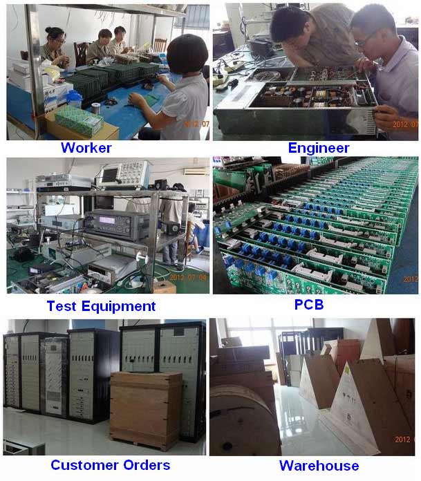
Our Factory

We have modernization of the factory . You are welcome to visit our factory when you come to China.

At present , there are already 1095 customers around the world visited our Guangzhou Tianhe office . If you come to China , you are welcome to visit us .
At Fair

This is our participation in 2012 Global Sources Hong Kong Electronics Fair . Customers from all over the world finally have a chance to get together.
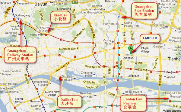
Where is Fmuser ?

You can search this numbers " 23.127460034623816,113.33224654197693 " in google map , then you can find our fmuser office .
FMUSER Guangzhou office is in Tianhe District which is the center of the Canton . Very near to the Canton Fair , guangzhou railway station, xiaobei road and dashatou , only need 10 minutes if take TAXI . Welcome friends around the world to visit and negotiate .
Contact: Sky Blue
Cellphone: +8618078869184
WhatsApp: +8618078869184
Wechat: +8618078869184
E-mail: [email protected]
QQ: 727926717
Skype: sky198710021
Address: No.305 Room HuiLan Building No.273 Huanpu Road Guangzhou China Zip:510620
|
|
|
|
English: We accept all payments , such as PayPal, Credit Card, Western Union, Alipay, Money Bookers, T/T, LC, DP, DA, OA, Payoneer, If you have any question , please contact me [email protected] or WhatsApp +8618078869184
-
PayPal.  www.paypal.com www.paypal.com
We recommend you use Paypal to buy our items ,The Paypal is a secure way to buy on internet .
Every of our item list page bottom on top have a paypal logo to pay.
Credit Card.If you do not have paypal,but you have credit card,you also can click the Yellow PayPal button to pay with your credit card.
---------------------------------------------------------------------
But if you have not a credit card and not have a paypal account or difficult to got a paypal accout ,You can use the following:
Western Union.  www.westernunion.com www.westernunion.com
Pay by Western Union to me :
First name/Given name: Yingfeng
Last name/Surname/ Family name: Zhang
Full name: Yingfeng Zhang
Country: China
City: Guangzhou
|
---------------------------------------------------------------------
T/T . Pay by T/T (wire transfer/ Telegraphic Transfer/ Bank Transfer)
First BANK INFORMATION (COMPANY ACCOUNT):
SWIFT BIC: BKCHHKHHXXX
Bank name: BANK OF CHINA (HONG KONG) LIMITED, HONG KONG
Bank Address: BANK OF CHINA TOWER, 1 GARDEN ROAD, CENTRAL, HONG KONG
BANK CODE: 012
Account Name : FMUSER INTERNATIONAL GROUP LIMITED
Account NO. : 012-676-2-007855-0
---------------------------------------------------------------------
Second BANK INFORMATION (COMPANY ACCOUNT):
Beneficiary: Fmuser International Group Inc
Account Number: 44050158090900000337
Beneficiary's Bank: China Construction Bank Guangdong Branch
SWIFT Code: PCBCCNBJGDX
Address: NO.553 Tianhe Road, Guangzhou, Guangdong,Tianhe District, China
**Note: When you transfer money to our bank account, please DO NOT write anything in the remark area, otherwise we won't be able to receive the payment due to government policy on international trade business.
|
|
|
|
* It will be sent in 1-2 working days when payment clear.
* We will send it to your paypal address. If you want to change address, please send your correct address and phone number to my email [email protected]
* If the packages is below 2kg,we will be shipped via post airmail, it will take about 15-25days to your hand.
If the package is more than 2kg,we will ship via EMS , DHL , UPS, Fedex fast express delivery,it will take about 7~15days to your hand.
If the package more than 100kg , we will send via DHL or air freight. It will take about 3~7days to your hand.
All the packages are form China guangzhou.
* Package will be sent as a "gift" and declear as less as possible,buyer don't need to pay for "TAX".
* After ship, we will send you an E-mail and give you the tracking number.
|
|
|
For Warranty .
Contact US--->>Return the item to us--->>Receive and send another replace .
Name: Liu xiaoxia
Address: 305Fang HuiLanGe HuangPuDaDaoXi 273Hao TianHeQu Guangzhou China.
ZIP:510620
Phone: +8618078869184
Please return to this address and write your paypal address,name,problem on note: |
|


