FPGA (Field-Programmable Gate Array), that is, field programmable gate array, is a product of further development on the basis of programmable devices such as PAL, GAL, and CPLD. It emerged as a semi-custom circuit in the field of application-specific integrated circuits (ASIC), which not only solves the deficiencies of custom circuits, but also overcomes the shortcomings of the limited number of gate circuits of the original programmable devices.
1. How FPGA works
FPGA adopts the concept of logic cell array LCA (Logic Cell Array), which includes three parts: Configurable Logic Block (CLB), IOB (Input Output Block), and Interconnect. A field programmable gate array (FPGA) is a programmable device. Compared with traditional logic circuits and gate arrays (such as PAL, GAL and CPLD devices), FPGA has a different structure. FPGA uses a small lookup table (16×1RAM) to implement combinational logic, and each lookup table is connected to a D flip-flop The flip-flops then drive other logic circuits or drive I/O to form a basic logic unit module that can realize both combinational logic functions and sequential logic functions. These modules are connected to each other or connected by metal wires. To the I/O module. FPGA logic is realized by loading programming data into the internal static storage unit. The value stored in the memory unit determines the logic function of the logic unit and the connection between modules or between modules and I/O, and finally determines The function that FPGA can realize, FPGA allows unlimited programming.
2. Basic Features
1) Using FPGA to design ASIC circuit (application-specific integrated circuit), users do not need to produce chips, and can get a suitable chip.
2) FPGA can be used as a sample chip for other fully customized or semi-customized ASIC circuits.
3) There are abundant flip-flops and I/O pins inside the FPGA.
4) FPGA is one of the devices with the shortest design cycle, the lowest development cost, and the lowest risk in ASIC circuits.
5) FPGA uses high-speed CMOS technology, low power consumption, and compatible with CMOS and TTL levels.
It can be said that FPGA chips are one of the best choices for small-batch systems to improve system integration and reliability.
FPGA is set by the program stored in the on-chip RAM to set its working state, therefore, it is necessary to program the on-chip RAM when working. Users can adopt different programming methods according to different configuration modes.
When power is on, the FPGA chip reads the data in EPROM into the on-chip programming RAM. After the configuration is completed, the FPGA enters the working state. After a power failure, the FPGA is restored to a blank, and the internal logic relationship disappears. Therefore, the FPGA can be used repeatedly. The programming of FPGA does not need a dedicated FPGA programmer, only general EPROM and PROM programmers. When you need to modify the FPGA function, you only need to change a piece of EPROM. In this way, the same piece of FPGA, different programming data, can produce different circuit functions. Therefore, the use of FPGA is very flexible.
3. FPGA configuration mode
FPGA has a variety of configuration modes: the parallel master mode is one FPGA plus one EPROM; the master-slave mode can support one PROM to program multiple FPGAs; the serial mode can use serial PROM to program the FPGA; the peripheral mode can use the FPGA as a micro The peripherals of the processor are programmed by the microprocessor. How to achieve fast timing closure, reduce power consumption and cost, optimize clock management and reduce the complexity of FPGA and PCB parallel design, etc., have always been key issues that system design engineers using FPGAs need to consider. Nowadays, as FPGAs develop toward higher density, larger capacity, lower power consumption, and more IP integration, system design engineers have to face the unprecedented performance and performance of FPGAs while benefiting from these excellent performances. New design challenges brought about by ability level. For example, the Virtex-5 series recently launched by leading FPGA manufacturer Xilinx uses a 65nm process and can provide up to 330,000 logic cells, 1,200 I/Os and a large number of hard IP blocks. Large capacity and density make complex wiring more unpredictable, which brings more serious timing closure problems. In addition, the greater number of logic functions, DSPs, embedded processing and interface modules integrated for different applications also make clock management and voltage distribution issues more difficult. Fortunately, FPGA vendors and EDA tool suppliers are working together to solve the unique design challenges of 65nm FPGAs. Not long ago, Synplicity and Xilinx announced the establishment of an ultra-large-capacity timing closure joint working group aimed at helping system design engineers to apply 65nm FPGA devices in a faster and more efficient manner. The synthesis tool Blast FPGA launched by design software supplier Magma can help establish an optimized layout and speed up timing closure. Recently, FPGA configuration methods have been diversified!


|
|
|
|
How far(long) the transmitter cover?
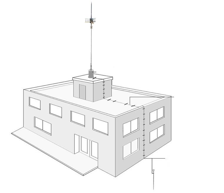
The transmission range depends on many factors. The true distance is based on the antenna installing height , antenna gain, using environment like building and other obstructions , sensitivity of the receiver, antenna of the receiver . Installing antenna more high and using in the countryside , the distance will much more far.
EXAMPLE 5W FM Transmitter use in the city and hometown:
I have a USA customer use 5W fm transmitter with GP antenna in his hometown ,and he test it with a car, it cover 10km(6.21mile).
I test the 5W fm transmitter with GP antenna in my hometown ,it cover about 2km(1.24mile).
I test the 5W fm transmitter with GP antenna in Guangzhou city ,it cover about only 300meter(984ft).
Below are the approximate range of different power FM Transmitters. ( The range is diameter )
0.1W ~ 5W FM Transmitter :100M ~1KM
5W ~15W FM Ttransmitter : 1KM ~ 3KM
15W ~ 80W FM Transmitter : 3KM ~10KM
80W ~500W FM Transmitter : 10KM ~30KM
500W ~1000W FM Transmitter : 30KM ~ 50KM
1KW ~ 2KW FM Transmitter : 50KM ~100KM
2KW ~5KW FM Transmitter : 100KM ~150KM
5KW ~10KW FM Transmitter : 150KM ~200KM
How to contact us for the transmitter?
Call me +8618078869184 OR
Email me [email protected]
1.How far you want to cover in diameter ?
2.How tall of you tower ?
3.Where are you from ?
And we will give you more professional advice.
About Us
FMUSER.ORG is a system integration company focusing on RF wireless transmission / studio video audio equipment / streaming and data processing .We are providing everything from advice and consultancy through rack integration to installation, commissioning and training.
We offer FM Transmitter, Analog TV Transmitter, Digital TV transmitter, VHF UHF Transmitter, Antennas, Coaxial Cable Connectors, STL, On Air Processing, Broadcast Products for the Studio, RF Signal Monitoring, RDS Encoders, Audio Processors and Remote Site Control Units, IPTV Products, Video / Audio Encoder / Decoder, designed to meet the needs of both large international broadcast networks and small private stations alike.
Our solution has FM Radio Station / Analog TV Station / Digital TV Station / Audio Video Studio Equipment / Studio Transmitter Link / Transmitter Telemetry System / Hotel TV System / IPTV Live Broadcasting / Streaming Live Broadcast / Video Conference / CATV Broadcasting system.
We are using advanced technology products for all the systems, because we know the high reliability and high performance are so important for the system and solution . At the same time we also have to make sure our products system with a very reasonable price.
We have customers of public and commercial broadcasters, telecom operators and regulation authorities , and we also offer solution and products to many hundreds of smaller, local and community broadcasters .
FMUSER.ORG has been exporting more than 15 years and have clients all over the world. With 13 years experience in this field ,we have a professional team to solve customer's all kinds of problems. We dedicated in supplying the extremely reasonable pricing of professional products & services. Contact email : [email protected]
Our Factory

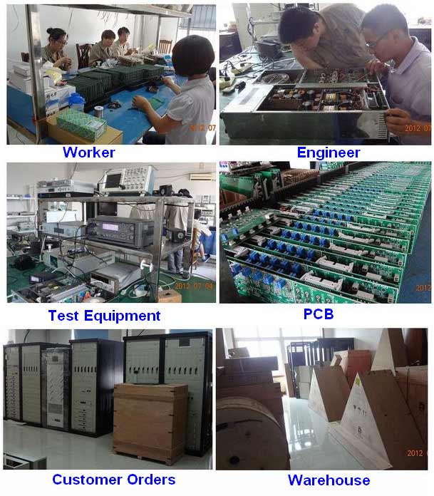
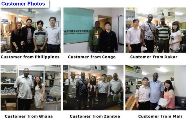
We have modernization of the factory . You are welcome to visit our factory when you come to China.

At present , there are already 1095 customers around the world visited our Guangzhou Tianhe office . If you come to China , you are welcome to visit us .
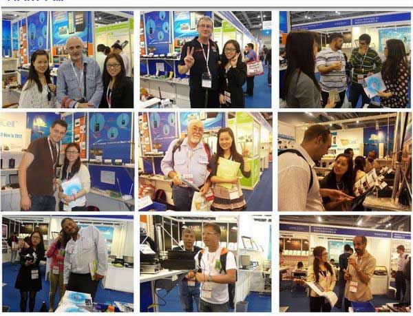
At Fair

This is our participation in 2012 Global Sources Hong Kong Electronics Fair . Customers from all over the world finally have a chance to get together.
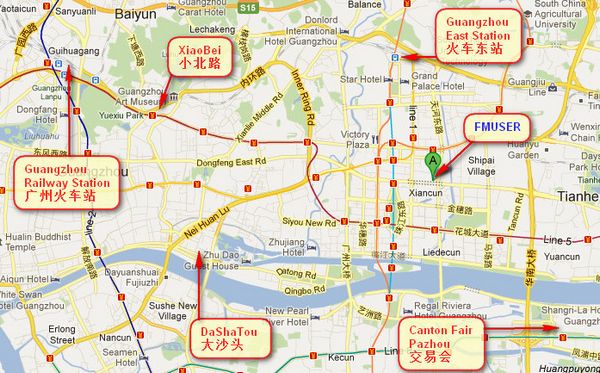
Where is Fmuser ?

You can search this numbers " 23.127460034623816,113.33224654197693 " in google map , then you can find our fmuser office .
FMUSER Guangzhou office is in Tianhe District which is the center of the Canton . Very near to the Canton Fair , guangzhou railway station, xiaobei road and dashatou , only need 10 minutes if take TAXI . Welcome friends around the world to visit and negotiate .
Contact: Sky Blue
Cellphone: +8618078869184
WhatsApp: +8618078869184
Wechat: +8618078869184
E-mail: [email protected]
QQ: 727926717
Skype: sky198710021
Address: No.305 Room HuiLan Building No.273 Huanpu Road Guangzhou China Zip:510620
|
|
|
|
English: We accept all payments , such as PayPal, Credit Card, Western Union, Alipay, Money Bookers, T/T, LC, DP, DA, OA, Payoneer, If you have any question , please contact me [email protected] or WhatsApp +8618078869184
-
PayPal.  www.paypal.com www.paypal.com
We recommend you use Paypal to buy our items ,The Paypal is a secure way to buy on internet .
Every of our item list page bottom on top have a paypal logo to pay.
Credit Card.If you do not have paypal,but you have credit card,you also can click the Yellow PayPal button to pay with your credit card.
---------------------------------------------------------------------
But if you have not a credit card and not have a paypal account or difficult to got a paypal accout ,You can use the following:
Western Union.  www.westernunion.com www.westernunion.com
Pay by Western Union to me :
First name/Given name: Yingfeng
Last name/Surname/ Family name: Zhang
Full name: Yingfeng Zhang
Country: China
City: Guangzhou
|
---------------------------------------------------------------------
T/T . Pay by T/T (wire transfer/ Telegraphic Transfer/ Bank Transfer)
First BANK INFORMATION (COMPANY ACCOUNT):
SWIFT BIC: BKCHHKHHXXX
Bank name: BANK OF CHINA (HONG KONG) LIMITED, HONG KONG
Bank Address: BANK OF CHINA TOWER, 1 GARDEN ROAD, CENTRAL, HONG KONG
BANK CODE: 012
Account Name : FMUSER INTERNATIONAL GROUP LIMITED
Account NO. : 012-676-2-007855-0
---------------------------------------------------------------------
Second BANK INFORMATION (COMPANY ACCOUNT):
Beneficiary: Fmuser International Group Inc
Account Number: 44050158090900000337
Beneficiary's Bank: China Construction Bank Guangdong Branch
SWIFT Code: PCBCCNBJGDX
Address: NO.553 Tianhe Road, Guangzhou, Guangdong,Tianhe District, China
**Note: When you transfer money to our bank account, please DO NOT write anything in the remark area, otherwise we won't be able to receive the payment due to government policy on international trade business.
|
|
|
|
* It will be sent in 1-2 working days when payment clear.
* We will send it to your paypal address. If you want to change address, please send your correct address and phone number to my email [email protected]
* If the packages is below 2kg,we will be shipped via post airmail, it will take about 15-25days to your hand.
If the package is more than 2kg,we will ship via EMS , DHL , UPS, Fedex fast express delivery,it will take about 7~15days to your hand.
If the package more than 100kg , we will send via DHL or air freight. It will take about 3~7days to your hand.
All the packages are form China guangzhou.
* Package will be sent as a "gift" and declear as less as possible,buyer don't need to pay for "TAX".
* After ship, we will send you an E-mail and give you the tracking number.
|
|
|
For Warranty .
Contact US--->>Return the item to us--->>Receive and send another replace .
Name: Liu xiaoxia
Address: 305Fang HuiLanGe HuangPuDaDaoXi 273Hao TianHeQu Guangzhou China.
ZIP:510620
Phone: +8618078869184
Please return to this address and write your paypal address,name,problem on note: |
|
