The purpose of RF budget analysis is to check the broadband frequency response and RF power level of different test points in the limiting amplifier. The analysis must be completed to correct for the worst-case operating temperature, gain slope, and wide RF input power range.
So, who knows what RF budget analysis is?
The basic layout of a limiting amplifier with a 40 dB limiting dynamic range is a cascade of four gain block amplifiers or LNAs. The ideal design uses only one or two dedicated amplifier devices to reduce power variation at different frequencies and minimize thermal/slope compensation requirements. Figure 1 shows the block diagram of the first initial limiting amplifiers before temperature correction and slope compensation.

Figure 1. Block diagram of preliminary design
First come a small benefit, recommend a technique to complete the design of broadband limiting amplifier:
1. Manage the limiting power dynamic range and eliminate RF overdrive conditions
2. Optimize performance within the temperature range
3. Finally, correct the power roll-off and flatten the small signal gain
4. The last minor correction may be necessary, that is, after the frequency equalization function is incorporated into the design, reconsider temperature compensation
Power limit
The main problem with the preliminary design shown in Figure 1 is that as the RF input power increases, RF overdrive is likely to occur at the output gain stage. When the saturated output power of any gain stage exceeds the absolute maximum input of the next amplifier in the queue, RF overdrive will occur. In addition, the design is prone to VSWR-related ripples, and oscillations are likely to occur due to the high undamped gain in the small RF package.
In order to prevent RF overdrive, eliminate VSWR effects and reduce the risk of oscillation, a fixed attenuator can be added between each gain stage to reduce power and gain. An RF absorber may also be required on the RF cover to eliminate oscillations. Sufficient attenuation is needed to reduce the maximum input power of each gain stage below the rated input power level of the MMIC. Sufficient attenuation must be included to accommodate the top input power margin, to accommodate temperature changes and differences between devices. Figure 2 shows where the RF attenuator is needed in the limiting amplifier chain.

Figure 2. RF overdrive correction block diagram
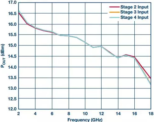
ADI's wideband limiting amplifier HMC7891 uses four HMC462 gain stages to allow the operating range to reach 10 dBm. The absolute maximum input power is 15 dBm. Each gain stage can tolerate a maximum RF input of 18 dBm. Following the design steps outlined in the previous paragraph, an attenuator has been added between the two gain stages to ensure that the maximum amplifier input power level does not exceed 17 dBm. Figure 3 shows the maximum power level at the input of each gain stage when a fixed attenuator is added to the design.

Figure 3. Simulation of the relationship between POUT and frequency, RF overdrive correction
The design is thermally compensated to expand the operating temperature range. The general thermal range requirement for limiting amplifier applications is -40°C to +85°C. Based on experience, the gain change formula of 0.01 dB/°/level can be used to estimate the gain change of a four-level amplifier design. The gain increases as the temperature decreases, and vice versa. Using the ambient gain as a baseline, the total gain is expected to decrease by 2.4 dB at 85°C and increase by 2.6 dB at –40°C.
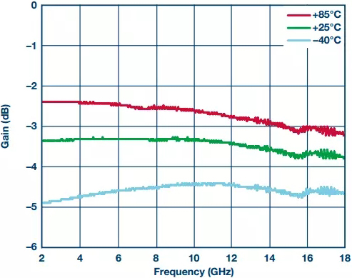
To thermally compensate the design, a commercially available Thermopad® temperature variable attenuator can be inserted to replace the fixed attenuator. Figure 4 shows the test results of a commercially available broadband Thermopad attenuator. Based on the Thermopad test data and estimated gain changes, it is obvious that two Thermopad attenuators are needed to thermally compensate the four-stage limiting amplifier design.

Figure 4. Thermopad loss over temperature
Deciding where to insert the Thermopad is an important decision. Because the loss of the Thermopad attenuator will increase, especially in low temperature conditions, it is a good practice to avoid adding components close to the output end of the RF chain in order to maintain a high limit output power level. The ideal location for the Thermopad is between the first three amplifier stages, which is the location highlighted in Figure 5.

Figure 5. Thermal compensation block diagram
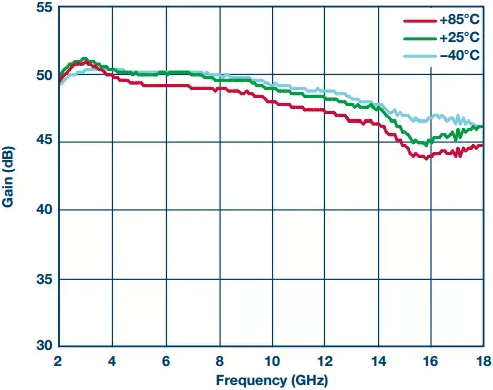
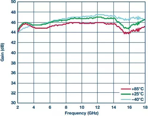
The simulation result of ADI's thermal compensation HMC7891 small signal performance is shown in Figure 6. Before frequency equalization, the gain change is reduced to a maximum of 2.5 dB. This is within the required range of ±1.5 dB gain change.

Figure 6. HMC7891 simulated small signal gain over temperature
Frequency equalization
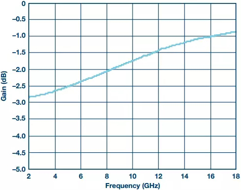
This compensates for the natural gain roll-off in most broadband amplifiers. There are various equalizer designs, including passive GaAs MMIC chips. Passive MMIC equalizers are small in size and have no DC and control signal requirements, so they are very suitable for limiting amplifier design. The number of frequency equalizers required depends on the uncompensated gain slope of the limiting amplifier and the response of the selected equalizer. A design recommendation is to slightly overcompensate the frequency response to offset transmission line loss and connector loss, as well as package parasitics that have a greater impact on gain at higher frequencies. Figure 7 shows the test results of the custom ADI GaAs frequency equalizer.

Figure 7. Measured frequency equalizer loss
ADI's HMC7891 limiting amplifier requires three frequency equalizers to correct the thermally compensated small signal response. Figure 8 shows the simulation results of HMC7891 after thermal compensation and frequency equalization. Deciding where to insert the equalizer is critical to a successful design. Before adding any equalizers, remember that an ideal limiting amplifier should evenly distribute the maximum amplifier compression between all gain stages to avoid excessive saturation. In other words, in the worst case, each MMIC should compress equally.

Figure 8. HMC7891 simulation frequency equalization small signal gain over temperature
In the current design stage shown in Figure 5, an equalizer connected in series with the Thermopad attenuator can be added at the input of the device to replace the fixed attenuator at the output of the device. Why did you do this? Four reasons
1. Adding an equalizer to the input of the limiting amplifier will reduce the power of the first gain stage. Therefore, the compression of level 1 is reduced. The reduction in gain stage compression is equivalent to the reduction in limiting dynamic range. In addition, due to the attenuation slope of the equalizer, the limiting dynamic range is dispersed in the frequency range. The lower the frequency, the more the dynamic range is reduced. To compensate for the reduced limiting dynamic range, the RF input power must be increased. However, due to the slope of the equalizer, an uneven increase in input power will increase the risk of overdrive of the amplifier gain stage. It is possible to add an equalizer to the input of the device, but this is not the ideal location.
2. Adding an equalizer connected in series with Thermopad will reduce the compression of subsequent amplifiers. This will result in uneven distribution of amplifier compression between gain stages, reducing the overall limiting dynamic range. It is not recommended to connect the equalizer in series with the Thermopad attenuator.
3. Using one or more equalizers instead of fixed attenuators will only change the compression level of the output stage amplifier. To minimize this variation and avoid RF overdrive, the equalizer loss should be roughly equal to the fixed attenuation value removed from the system. In addition, as mentioned above, adding an equalizer before the gain stage will result in a dispersion of the limiting dynamic range and frequency. To minimize this effect, replace as few equalizers as possible.
4. The equalizer can be added to the output of the device. Output equalization will reduce the output power, but will not produce limiting dynamic range dispersion. Output equalization produces a slightly positive output power slope, but this slope is offset by high-frequency packaging and connector losses.
The finished four-stage limiting amplifier layout is shown in Figure 9.

Figure 9. Block diagram of frequency equalization
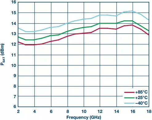
Figure 10 shows the output power and temperature simulation results of ADI HMC7891. The final design achieved a limiting dynamic range of 40 dB. Under all operating conditions, the simulated worst-case output power change was 3 dB.

Figure 10. The relationship between simulated PSAT of HMC7891 and frequency within the temperature range
Our other product:


