LDMOS (Laterally Diffused Metal Oxide Semiconductor) is developed for 900MHz cellular phone technology. The continuous growth of the cellular communication market ensures the application of LDMOS transistors, and also makes LDMOS technology continue to mature and costs continue to decrease, so It will replace bipolar transistor technology in most cases in the future. Compared with bipolar transistors, the gain of LDMOS tubes is higher. The gain of LDMOS tubes can reach more than 14dB, while that of bipolar transistors is 5~6dB. The gain of PA modules using LDMOS tubes can reach about 60dB. This shows that fewer devices are required for the same output power, thereby increasing the reliability of the power amplifier.
LDMOS can withstand a standing wave ratio three times higher than that of a bipolar transistor, and can operate at a higher reflected power without destroying the LDMOS device; it can withstand the over-excitation of the input signal and is suitable for transmitting digital signals, because it has Advanced instantaneous peak power. The LDMOS gain curve is smoother and allows multi-carrier digital signal amplification with less distortion. The LDMOS tube has a low and unchanged intermodulation level to the saturation region, unlike bipolar transistors that have a high intermodulation level and change with the increase of power level. This main feature allows LDMOS transistors to perform twice as much power as bipolar transistors with better linearity. LDMOS transistors have better temperature characteristics and the temperature coefficient is negative, so the influence of heat dissipation can be prevented. This kind of temperature stability allows the amplitude change to be only 0.1dB, and in the case of the same input level, the amplitude of the bipolar transistor changes from 0.5 to 0.6dB, and a temperature compensation circuit is usually required.
LDMOS structure characteristics and advantages of use
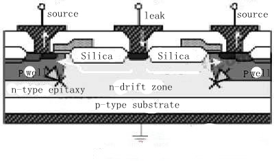
LDMOS is widely adopted because it is easier to be compatible with CMOS technology. The LDMOS device structure is shown in Figure 1. LDMOS is a power device with a double diffused structure. This technique is to implant twice in the same source/drain region, one implantation of arsenic (As) with a larger concentration (typical implantation dose of 1015cm-2), and another implantation of boron (with a smaller concentration (typical implantation dose of 1013cm-2)). B). After the implantation, a high-temperature propulsion process is carried out. Since boron diffuses faster than arsenic, it will diffuse further along the lateral direction under the gate boundary (P-well in the figure), forming a channel with a concentration gradient, and its channel length Determined by the difference between the two lateral diffusion distances. In order to increase the breakdown voltage, there is a drift region between the active region and the drain region. The drift region in LDMOS is the key to the design of this type of device. The impurity concentration in the drift region is relatively low. Therefore, when the LDMOS is connected to a high voltage, the drift region can withstand a higher voltage due to its high resistance. The polycrystalline LDMOS shown in Fig. 1 extends to the field oxygen in the drift region and acts as a field plate, which will weaken the surface electric field in the drift region and help increase the breakdown voltage. The effect of the field plate is closely related to the length of the field plate. To make the field plate fully functional, one must design the thickness of the SiO2 layer, and second, the length of the field plate must be designed.
The LDMOS manufacturing process combines BPT and gallium arsenide processes. Different from the standard MOS process, in the device packaging, LDMOS does not use BeO beryllium oxide isolation layer, but is directly hard-wired on the substrate. The thermal conductivity is improved, the high temperature resistance of the device is improved, and the device life is greatly extended. . Due to the negative temperature effect of the LDMOS tube, the leakage current is automatically evened when heated, and the positive temperature effect of the bipolar tube does not form a local hot spot in the collector current, so that the tube is not easily damaged. So LDMOS tube greatly strengthens the bearing capacity of load mismatch and overexcitation. Also due to the automatic current sharing effect of the LDMOS tube, its input-output characteristic curve curves slowly at the 1dB compression point (saturation section for large signal applications), so the dynamic range is widened, which is conducive to the amplification of analog and digital TV RF signals. LDMOS is approximately linear when amplifying small signals with almost no intermodulation distortion, which simplifies the correction circuit to a great extent. The DC gate current of the MOS device is almost zero, the bias circuit is simple, and there is no need for a complex active low-impedance bias circuit with positive temperature compensation.
For LDMOS, the thickness of the epitaxial layer, the doping concentration, and the length of the drift region are the most important characteristic parameters. We can increase the breakdown voltage by increasing the length of the drift region, but this will increase the chip area and on-resistance. The withstand voltage and on-resistance of high-voltage DMOS devices depend on a compromise between the concentration and thickness of the epitaxial layer and the length of the drift region. Because withstand voltage and on-resistance have contradictory requirements for the concentration and thickness of the epitaxial layer. A high breakdown voltage requires a thick lightly doped epitaxial layer and a long drift region, while a low on-resistance requires a thin heavily doped epitaxial layer and a short drift region. Therefore, the best epitaxial parameters and drift region must be selected Length in order to obtain the smallest on-resistance under the premise of meeting a certain source-drain breakdown voltage.
LDMOS has outstanding performance in the following aspects:
1. Thermal stability; 2. Frequency stability; 3. Higher gain; 4. Improved durability; 5. Lower noise; 6. Lower feedback capacitance; 7. Simpler bias current circuit; 8 . Constant input impedance; 9. Better IMD performance; 10. Lower thermal resistance; 11. Better AGC capability. LDMOS devices are particularly suitable for CDMA, W-CDMA, TETRA, digital terrestrial television and other applications that require a wide frequency range, high linearity and high service life requirements.
LDMOS was mainly used for RF power amplifiers in mobile phone base stations in the early days, and can also be applied to HF, VHF and UHF broadcast transmitters, microwave radars and navigation systems, and so on. Exceeding all RF power technologies, Laterally Diffused Metal Oxide Semiconductor (LDMOS) transistor technology brings higher power peak-to-average ratio (PAR, Peak-to-Aerage), higher gain and linearity to the new generation of base station amplifiers At the same time, it brings higher data transmission rate for multimedia services. In addition, excellent performance continues to increase with efficiency and power density. In the past four years, Philips' second-generation 0.8-micron LDMOS technology has dazzling performance and stable mass production capacity on GSM, EDGE and CDMA systems. At this stage, in order to meet the requirements of multi-carrier power amplifiers (MCPA) and W-CDMA standards, An updated LDMOS technology is also provided.
Our other product:


