I have done RF research and development work for many years, and I have been engaged in RF chip support work at Runxin Technology for 7 years. As for the design experience of RF circuits, I will share with you here. I hope that the content of the following talks will be useful for RF design work. The engineers from here will be a little helpful, so let’s keep the gossip and go straight to the topic. Let's take a look at the relevant content along with the analog electronic editor.
The reference design of the EVB board allows us to get twice the result with half the effort
When we design a brand-new RF chip and require us to quickly understand the performance indicators of the RF part of the chip and the requirements for peripheral devices, and to do the design work of this part quickly, our most important need is What we do is to carefully read and understand the chip specifications and the design and precautions of the reference board. This plays a key role in the success or failure of our first edition design, especially some RF chips and some specific RF devices on the RF periphery. (Such as PA LNA BPF, etc.) It is especially important to cooperate with this one.
Let's look at a case of the RF circuit in the figure below:
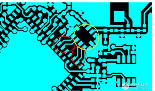
This circuit is a circuit that cooperates with a high-performance RF chip and an integrated BALUN (the IC in the yellow part of the picture above). Since there is no matching circuit between the main chip and BALUN, this part is entirely based on the line width and line length of the RF trace. And the impedance control of the differential signal is matched, and it cannot be debugged by the peripheral components later. Therefore, there are strict requirements for the wiring of the differential part (as shown in the red part of the figure above). The quality of the wiring and impedance control directly affects the entire RF Part of the post-debugging indicators are good or bad, so the design requirements for the EVB board of the RF chip must be referenced in the early design stage, so that it can get twice the result with half the effort.
In the design process of many of our projects, the design cost will be an important part of our design process. The cost of our RF circuit part is mainly based on whether the peripheral circuit is built with discrete components or integrated IC. Peripheral RF Part of the use of integrated circuits will be more expensive to build than using separate devices, so here we mainly talk about what matters to pay attention to in the peripheral circuits of separate devices.
The following figure is a partial circuit of a path in a certain design:
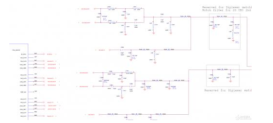
Since the peripherals are all circuits built with capacitors and inductors, the layout of this part of the circuit becomes more important under the premise that our board size requirements are getting smaller and smaller.
1. The RF components should be placed on the same layer as much as possible, and try to avoid punching the RF traces to the other side. This layout is mainly to reduce the risk of RF indicator problems caused by the PCB board punching.
2. Considering the integrity of the RF trace and grounding, if a large packaged device cannot be guaranteed, try to use a small packaged device to save more space and complete the grounding.
3. If there are multiple circuits of WLAN, BLE, Zigbee in the designed circuit, the mutual interference and coexistence of multiple signals require us to consider the layout of the wiring at the early stage of the design, and try to make the layout of the wiring and device placement to ensure safety Distance, reducing our uncontrollable requirements for the product's later performance.
All the hard work in the early stage of circuit design is to make the product a qualified product. For RF products, process control is particularly important. The specifics are as follows:
1. PCB process, the RF board has strict requirements for the impedance control of the PCB board and the RF part of the trace. The requirements of the RF trace impedance of 50 ohms and the differential impedance of 100 ohms need to be confirmed with the PCB board manufacturer whether the board manufacturer can do it, and try to Have done RF PCB board factory to make boards.
2. The pre-commissioning has requirements for the brand of materials used, and the brand of the commissioned materials and mass-produced materials must be consistent.
3. For the requirements of PCB suppliers, the preliminary R&D proofing and mass production ensure that the PCB manufacturers are consistent. If you want to import multiple PCB suppliers, you need to verify the RF indicators of the PCB boards provided by different manufacturers.
RF circuit design work requires R&D engineers to have a long-term work accumulation. There is no shortcut to find. An excellent RF engineer must have rich experience in RF product R&D and debugging. This article is only used as some of my work experience, there are more RF solutions, you can directly pay attention to Runxin Technology, Runxin Technology has been focusing on RF solutions for many years, and has cooperated with many large enterprises at home and abroad. Welcome to everyone Communicate together.
Our other product:


