In recent years, with the rapid development of computers, digital networks, and television technologies, people’s demand for high-quality television images has continued to increase, and my country’s radio and television industry has undergone rapid development and rapid development. The digital TV satellite broadcasting, which was launched four years ago, has now formed a considerable scale. Digital video recording, digital special effects, non-linear editing systems, virtual studios, digital broadcast vehicles, network hard disk arrays, and robotic digital playback systems have successively entered CCTV and provincial and municipal TV stations. The standard high-definition digital TV SDTV/HDTV has been listed as a major national scientific research industry project, and the pilot broadcast has been carried out on the Central Radio and Television Tower. At present, my country's digital television program production and digital television terrestrial broadcasting have been intensively promoted, and the "Eleventh Five-Year Plan" will be the preparation period for the overall shift of my country's digital television, and an important stage of the transition of the broadcasting and television system from analog to digital.
This design is designed to cope with this trend and to meet the huge market demand for multi-channel ASI/SDI digital video signal optical transmission equipment. It is an optical transmission equipment that uses time division multiplexing technology to simultaneously transmit two ASI/SDI digital video signals in an optical fiber. This design can lay a solid foundation for the development of more high-speed asynchronous digital signal optical transmission equipment in the future.
1. System implementation plan
The ASI/SDI serial signal is reshaped by the equalization circuit and converted into a set of differential signals; then the clock in the signal is extracted through the clock recovery circuit for use in the next decoding and synchronization of the signal; after passing through the decoding circuit , The serial high-speed signal is transformed into a parallel low-speed signal to prepare for the next electrical multiplexing process; finally, the asynchronous signal is synchronized with the local electrical multiplexing clock through the adjustment of the FIFO circuit, thereby realizing the local electrical multiplexing ; It is then transmitted to the receiving end through the electrical/optical conversion of the optical module. After receiving the signal, the receiving end passes through a series of inverse conversion circuits to restore the original ASI/SDI serial signal to complete the entire transmission process.
In this design, the electrical multiplexing technology of ASI/SDI signals is the key to the entire technical link. Because the ASI/SDI signal rate required for power multiplexing in the project is very high, the standard rate reaches 270Mbit/s, and it is not a homologous signal multiplexing, it is difficult and uneconomical to directly multiplex the signal, and it needs to be restored first. The clock of each signal converts the high-speed serial signal into a low-speed parallel signal, and then adjusts the clock pace of each signal through the FIFO chip circuit to achieve synchronization with the local clock, and then multiplexes the two electrical signals through the programmable chip , And then realize the time division multiplex transmission. Only after this series of signal processing procedures can a smooth demultiplexing process be realized at the receiving end, which is also the main technical point of the design.
In addition, the locking of electrical multiplexing is also a problem. The more signal channels, the higher the speed, the more difficult it is to lock, and the higher the technical requirements for the layout of the PCB board. This problem can be solved very well through various treatments such as reasonable placement of various components and scientific filtering of clutter.
2. Hardware circuit
In this design, the main use is the latest powerful and stable digital video chipset from National Semiconductor. The decoding and serial/parallel conversion chip is CLC011; the encoding and parallel/serial conversion chip is CLC020; the clock recovery chip is LMH0046; the adaptive cable equalization chip is CLC014; the CPLD chip is LC4256V from LATTICE; the FIFO chip is IDT72V2105 from IDT.
Equalization part of the circuit processing process is shown in Figure 2. It can be seen from Figure 2 that the single-ended input ASI/SDI serial signal is reshaped after passing through the equalization circuit and converted into a set of differential signals, which is ready for the subsequent clock recovery process. After passing the equalization circuit, the signal quality is greatly improved, and the input and output signal waveforms are compared as shown in Figure 3.
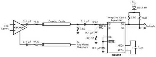
Figure 2 Balancing part of the circuit processing process
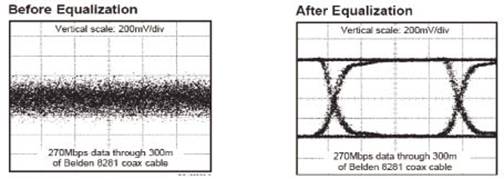
Figure 3 Waveform comparison of equalization circuit
The clock recovery part of the circuit processing process is shown in Figure 4. It can be seen from Figure 4 that the working mode of the chip is correctly set, a 27M clock is provided locally for the clock recovery chip to use, the balanced high-speed differential signal is input to the chip, and the serial signal is recovered after the chip is processed The clock signal in it is used by the following decoding part of the circuit. At the same time, the chip can also support clock recovery for high-definition signals.
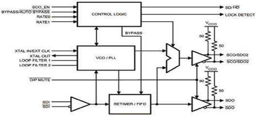
Figure 4 Clock recovery part of the circuit processing process
The process of decoding part of the circuit is shown in Figure 5. It can be seen from Figure 5 that the serial clock and serial data recovered by the clock recovery chip are input to the decoding chip, after serial/parallel conversion, 10-bit parallel data and 27M parallel clock are output to prepare the clock for the following FIFO circuit Adjust the use. The timing diagram of the signals in each working mode is shown in Fig. 6.
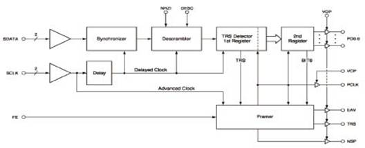
Figure 5 Decoding part of the circuit processing process
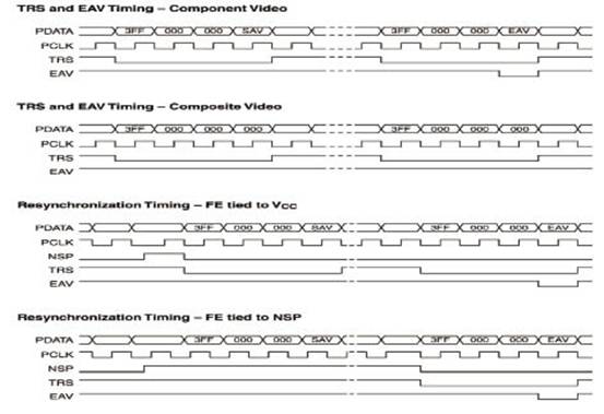
Figure 6 Signal timing diagram of each mode
The FIFO part of the circuit processing process is shown in Figure 7. Among them, the read clock uses the 27M parallel clock recovered by the encoding circuit, and the write clock uses the local 27M clock. The 10-bit parallel signal passing through the FIFO is synchronized with the local clock through adjustment to prepare for the subsequent input to the CPLD for electrical multiplexing. The electric multiplexing procedure of CPLD is as follows, among which 2BP-S is the multiplexing procedure, and 2BS-P is the demultiplexing procedure.
Figure 7 FIFO part of the circuit processing process
Architecture SCHEMATIC of 2BP-S is
SIGNAL gnd: std_logic := '0';
SIGNAL vcc: std_logic := '1';
Signal N_25: std_logic;
Signal N_12: std_logic;
Signal N_13: std_logic;
Signal N_15: std_logic;
Signal N_16: std_logic;
Signal N_17: std_logic;
Signal N_21: std_logic;
Signal N_22: std_logic;
Signal N_23: std_logic;
Signal N_24: std_logic;
Begin
I30: G_D Port Map (CLK=>N_25, D=>N_13, Q=>N_22 );
I29: G_D Port Map (CLK=>N_25, D=>N_16, Q=>N_23 );
I34: G_OUTPUT Port Map (I=>N_22, O=>Q0 );
I33: G_OUTPUT Port Map (I=>N_23, O=>Q1 );
I2: G_INPUT Port Map (I=>CLK, O=>N_25 );
I7: G_INPUT Port Map (I=>A, O=>N_12 );
I8: G_INPUT Port Map (I=>LD, O=>N_21 );
I6: G_INPUT Port Map (I=>B, O=>N_15 );
I12: G_2OR Port Map (A=>N_17, B=>N_24, Y=>N_16 );
I16: G_2AND1 Port Map (AN=>N_21, B=>N_22, Y=>N_24 );
I21: G_2AND Port Map (A=>N_21, B=>N_12, Y=>N_13 );
I20: G_2AND Port Map (A=>N_21, B=>N_15, Y=>N_17 );
End SCHEMATIC;
Architecture SCHEMATIC of 2BS-P is
SIGNAL gnd: std_logic := '0';
SIGNAL vcc: std_logic := '1';
Signal N_5: std_logic;
Signal N_1: std_logic;
Signal N_3: std_logic;
Signal N_4: std_logic;
Begin
I8: G_OUTPUT Port Map (I=>N_4, O=>Q0 );
I1: G_OUTPUT Port Map (I=>N_5, O=>Q1 );
I2: G_INPUT Port Map (I=>CLK, O=>N_3 );
I3: G_INPUT Port Map (I=>SIN, O=>N_1 );
I7: G_D Port Map (CLK=>N_3, D=>N_4, Q=>N_5 );
I4: G_D Port Map (CLK=>N_3, D=>N_1, Q=>N_4 );
End SCHEMATIC;
The coding part of the circuit processing process is shown in Figure 8. After receiving the data, the receiving optical module recovers the parallel data and synchronous clock through the demultiplexing program of the CPLD, and then recovers the original high-speed serial signal through the encoding chip circuit, which is finally output by the transmission device after being driven by the cable driver chip. Complete the entire transfer process. Among them, the signal sequence of the encoding circuit part is shown in Figure 9.
Figure 8 Code part of the circuit processing process
Figure 9 Signal timing diagram of encoding circuit
3. concluding remarks
The design of the CPLD-based asynchronous ASI/SDI signal electrical multiplexing optical transmission equipment uses the latest ASI/SDI signal electrical multiplexing/demultiplexing technology, which can realize the time division multiplexing transmission of two signals, replacing the previous wave division multiplexing The technology-based multi-channel asynchronous signal transmission mode greatly saves production costs and further improves the market competitiveness of products.
Our other product:


