In recent years, digital video surveillance systems have been widely used in various fields such as banks, highways, and buildings. In digital video surveillance systems, OSD (On Screen Display) technology is an indispensable part. OSD provides users with a friendly man-machine interface, enabling users to obtain more additional information.
1. System composition
The system introduced in this article is a complete video surveillance system based on TI DSP TMS320DM6? 3 and FPGA. It supports 1 channel of video input and 1 channel of video output, and also provides a network interface.
Video input is realized by TI’s cost-effective video decoder TVP5150A. TVP5150A can realize the collection of two composite video inputs or one S-video video signal. The register is configured through I2C, and the output digital video signal follows the ITU656 standard.
The digital video signal decoded by TVP5150A is transmitted to the DSP through the video port 1 of DM6? 3, and the necessary video processing is performed by the DSP, and then output to the remote device by the network interface. On the other hand, after DM6? 3 processes the video data received from the network, it is displayed and output by SAA7105 through video port 2 through FPGA.
The output part is realized by SAA7105. SAA7105 is a high-performance video encoder of NXP Company, which can provide composite video output, VGA video output and HDTV high-definition video signal output. The control of SAA7105 is also realized through I2C, and it receives the digital video signal of composite ITU656 standard.
The video processing part adopts TI's DSP TMS320DM6 3 to realize. The main frequency of DM6?3 can reach 600MHz, and there are two 20-bit video ports. The video ports support digital video interfaces such as BT.656 and Y/C. DM6?3 also integrates network MAC to realize network access.
The development speed of hardware performance is always difficult to meet the needs of software. In the increasingly complex applications of video processing, DSP is responsible for complex video processing tasks, and resources become very tight. Therefore, in the design of this system, FPGA is used to realize the design of OSD, which can reduce the burden of DSP.
The OSD implementation part uses Xilinx's XC3S250E. XC3S250E is a Xilinx SPARTAN-3E series FPGA with 250,000 logic gates.
2. OSD implementation
SAA7105 cannot realize OSD function, but is realized by XC3S250E. The main control chip DM6? 3 only needs to inform the FPGA of the content and position to be displayed, and the specific work is performed by the FPGA. The logical block diagram of OSD is shown as in Fig. 2.
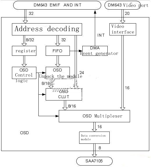
OSD FPGA receives OSD data and control instructions from DSP DM6 3 through EMIFA, receives video data through DSP video port 1, and superimposes OSD information on the video data, and outputs it to the video encoder SAA7105. The functional modules of OSD are described as follows.
The data port of the address decoding module is interfaced with the low 32-bit data of EMIFA of DSP DM6 3, and receives the data and control information sent by DM6 3. These data and control information are the original 32-bit data sent by DM6 3. The address decoding module puts the received OSD data, such as the content of the OSD, into the internal FIFO of the FPGA in a 32-bit data format. The control information is mainly used to control the OSD through a set of control registers.
There is also a video interface module directly connected to the DSP. The video interface module is connected to the video port 2 of the DSP, and stores the data and control information from the DSP video port. These control information are directly transmitted to the OSD multi-channel control module, and the control information also directly controls the video decoder SAA7105.
The OSD control logic outputs the control information obtained from the control register group to each functional module of the OSD to realize the control of the OSD. The register group is mainly divided into two parts: one is the asynchronous register group, which sends control information such as reset, OSD enable and select data width to the OSD; the other is the synchronous register group, which mainly controls the position information of the OSD.
The OSD decoding module takes out the data to be displayed from the FIFO according to the control information of the control logic, and outputs it to the OSD CLUT module in synchronization with the video data. The data obtained from the FIFO is the original DSP 32-bit data, and the data required by the OSD CLUT module is 8/16-bit, so the OSD unpacking module needs to unpack the 32-bit data according to the frequency of the video port. The 32-bit data is transmitted to the OSD CLUT module with a width of 8/16.
Another function of the FIFO module is to transfer FIFO status information to the DMA event generator module, such as FIFO full or FIFO empty. The DMA event generator monitors these events, and if they occur, they are sent to DM6? 3 in an interrupt mode to achieve correct read and write operations to the FIFO.
The OSD CLUT module searches for the corresponding value of YCbCr for the data of each pixel received from the OSD unpacking module, and controls the output sequence of these OSD CLUT data. This conversion relationship is transmitted by the DSP through the 24-bit data port. The data of the OSD CLUT module is directly output to the OSD multi-channel controller module.
The OSD multi-channel control module determines the output video data according to the Alpha control bit received from the OSD CLUT module. If the current OSD information, that is, the Alpha control bit is valid, it outputs the OSD data to the data conversion module. Otherwise, output the original video data received from the video interface module to realize the OSD function.
The data output by the OSD multi-channel controller is not directly sent to the video decoder, but through the data conversion module, according to specific application conditions, the necessary data format conversion is performed. It can be seen from the interface timing of SAA7105 that when SAA7105 is configured for composite video output, the required data is single clock edge data. At this time, the data conversion module does not do any work, and the data received from the OSD multi-channel control module is transmitted intact. For SAA7105; if SAA7105 is configured in VGA or HDTV output mode, dual clock edge data is required. At this time, the data conversion module converts the single clock edge data received from the OSD controller into dual clock edge data and outputs it to the video decoder SAA7105 .
It can be seen that FPGA has completed all the work of OSD. If you want to display the OSD content, DM6? 3 only needs to send control instructions to the FPGA through the EMFIA port. These instructions, of course, include the content and location information of the OSD.
3. OSD control
The OSD design implemented by XC3S250E performs OSD display based on the received OSD location and content information, without any restrictions on the content displayed by the OSD, which is very flexible and convenient. The following takes OSD Chinese character display as an example to illustrate the control operation of OSD.
To display Chinese characters correctly, the input Chinese character internal code must be converted into the corresponding location code. For this function, we use the function Uint32 Code_Converse(unsigned char *CodeNPointer), whose input is a pointer, pointing to the Chinese character to be converted. The return value is the location code corresponding to the Chinese character. OSD display is realized by the function OSDHZ?isplay:
void OSDHZ_ Display{
Uint8 *pFrame
Uint32 pitch
OSDUTIL_Point* loc
Uint32 CodeQ
OSDHZ?ont *font
Uint8 fgColor
Uint8 bgColor
}
Among them, Uint8 *pFrame is the Buffer buffer for OSD output; Uint32 pitch is the pixel value displayed in each line; OSDUTIL_Point *loc is the display position of the first character; Uint32 CodeQ is the area code to display Chinese characters; OSDHZ?ont * font is the font used to display Chinese characters; Uint8 fgColor displays the foreground color of Chinese characters; Uint8 bgColor displays the background color of Chinese characters.
Therefore, if you need to display Chinese characters, you only need to convert the Chinese characters to the necessary code system, and then output the converted area code to the OSD FPGA. Of course, to display Chinese characters, the Chinese character library is indispensable.
Our other product:


