OLED (Organic light emitTIng diode) is a new generation of flat panel display technology following TFT-LCD (Thin film transistor liquid crystal display). It has the advantages of simple structure, no need for a backlight for self-luminescence, high contrast, thin thickness, wide viewing angle, fast response speed, can be used for flexible panels, and a wide operating temperature range. In 1987, Dr. C.W. Tang and others from Kodak Corporation of the United States established OLED components and basic materials [1]. In 1996, Pioneer of Japan became the first company to mass-produce this technology, and matched the OLED panel to the car audio display it produced. In recent years, due to its promising prospects, R&D teams in Japan, the United States, Europe, Taiwan and South Korea have sprung up, leading to the maturity of organic light-emitting materials, the vigorous development of equipment manufacturers, and the continuous evolution of process technology.
However, OLED technology is related to the current mature semiconductor, LCD, CD-R or even LED industries in terms of principles and processes, but has its unique know-how; therefore, there are still many bottlenecks in the mass production of OLED. . Taiwan Rebao Technology Co., Ltd. began to develop OLED-related technologies in 1997 and successfully mass-produced OLED panels in 2000. It became the second mass-produced OLED panel company in the world after Tohoku Pioneer in Japan; and in 2002, it continued to produce OLED panels. The mono-color and area-color panels for export shipments are shown in Figure 1, and the yield and output have been increased, making it the world's largest OLED panel supplier in terms of output.
In the OLED process, the thickness of the organic film layer will greatly affect the characteristics of the device. Generally speaking, the thickness error of the film must be less than 5 nanometers, which is a veritable nanotechnology. For example, the third-generation substrate size of TFT-LCD flat panel displays is generally defined as 550mm x 650mm. On a substrate of this size, it is difficult to control such a precise film thickness. The process of area substrate and the application of large area panel. Currently, OLED applications are mainly small mono-color and area-color display panels, such as mobile phone main screens, mobile phone secondary screens, game console displays, car audio screens, and personal Digital Assistant (PDA) display. Since the mass production process of OLED full-color has not yet matured, small-size full-color OLED products are expected to be launched in succession after the second half of 2002. Since OLED is a self-luminous display, its visual performance is extremely excellent compared to full-color LCD displays of the same level. It has the opportunity to directly cut into full-color small-size high-end products, such as digital cameras and palm-sized VCD (or DVD) players. As for large panels (13 inches or more), although there is a research and development team showing samples, the mass production technology is still to be developed.
OLEDs are generally divided into small molecules (usually called OLED) and macromolecules (usually called PLED) due to different light-emitting materials. The technology licenses are Eastman Kodak (Kodak) in the United States and CDT (Cambridge Display Technology) in the United Kingdom. Taiwan Rebao Technology Co., Ltd. is one of the few companies that simultaneously develops OLED and PLED. In this article, we will mainly introduce small molecule OLEDs. First, we will introduce the principle of OLED, then we will introduce related key processes, and finally we will introduce the current development direction of OLED technology.
1. Principle of OLED
OLED components are composed of n-type organic materials, p-type organic materials, cathode metal and anode metal. Electrons (holes) are injected from the cathode (anode), are conducted to the light-emitting layer (generally n-type material) through the n-type (p-type) organic material, and emit light through recombination. Generally speaking, ITO is sputtered on a glass substrate made of an OLED device as an anode, and then a p-type and n-type organic material and a low work function metal cathode are sequentially deposited by vacuum thermal evaporation. Because organic materials easily interact with water vapor or oxygen, dark spots are generated and the components do not shine. Therefore, after the vacuum coating of this device is completed, the packaging process must be performed in an environment without moisture and oxygen.
Between the cathode metal and the anode ITO, the widely used device structure can generally be divided into 5 layers. As shown in Figure 2, from the side close to the ITO, they are: hole injection layer, hole transport layer, light-emitting layer, electron transport layer, and electron injection layer. Regarding the evolution history of OLED devices, the OLED device first published by Kodak in 1987 is composed of two layers of organic materials, a hole transport layer and an electron transport layer. The hole transport layer is a p-type organic material, which is characterized by higher hole mobility, and its highest occupied molecule orbital (HOMO) is closer to ITO, allowing holes to be transferred from The energy barrier of ITO injected into the organic layer is reduced.
As for the electron transport layer, it is an n-type organic material, which is characterized by high electron mobility. When electrons travel from the electron transport layer to the interface of the hole and electron transport layer, the lowest non-occupied molecular orbital of the electron transport layer The lowest unoccupied molecule orbital (LUMO) is much higher than the LUMO of the hole transport layer. It is difficult for electrons to cross this energy barrier to enter the hole transport layer and are blocked by this interface. At this time, holes are transferred from the hole transport layer to the vicinity of the interface and recombine with electrons to generate excitons (Exciton), and Exciton releases energy in the form of light emission and non-light emission. In terms of a general Fluorescence material system, only 25% of the electron-hole pairs are recombined in the form of light emission based on the calculation of the selectivity (SelecTIon rule), and the remaining 75% of the energy is the result of heat release. Dissipated form. In recent years, phosphorescence (Phosphorescence) materials are being actively developed to become a new generation of OLED materials [2], such materials can break the limit of selectivity to increase the internal quantum efficiency to nearly 100%.
In the two-layer device, the n-type organic material-the electron transport layer-is also used as the light-emitting layer, and the light-emitting wavelength is determined by the energy difference between HOMO and LUMO. However, a good electron transport layer—that is, a material with high electron mobility—is not necessarily a material with good light emission efficiency. Therefore, the current general practice is to dope (doped) high-fluorescence organic pigments for electron transport. The part of the layer close to the hole transport layer, also known as the light-emitting layer [3], has a volume ratio of about 1% to 3%. The development of doping technology is a key technology used to enhance the fluorescence quantum absorption rate of raw materials. Generally, the selected material is a dye with high fluorescence quantum absorption rate (Dye). Since the development of organic dyes originated from dye lasers in the 1970s to 1980s, the material system is complete, and the emission wavelength can cover the entire visible light region. The energy band of the organic dye doped in the OLED device is poor, generally smaller than the energy band of the host (Host), in order to facilitate the exciton energy transfer from the host to the dopant (Dopant). However, because the dopant has a small energy band and acts as a trap in electrical terms, if the dopant layer is too thick, the driving voltage will increase; but if it is too thin, the energy will be transferred from the host to the dopant. The ratio will get worse, so the thickness of this layer must be optimized.
The metal material of the cathode traditionally uses a metal material (or alloy) with low work function, such as magnesium alloy, to facilitate the injection of electrons from the cathode to the electron transport layer. In addition, a common practice is to introduce an electron injection layer. It is composed of a very thin low work function metal halide or oxide, such as LiF or Li2O, which can greatly reduce the energy barrier between the cathode and the electron transport layer [4] and reduce the driving voltage.
Since the HOMO value of the hole transport layer material is still different from that of ITO, in addition, after a long time operation, the ITO anode may release oxygen and damage the organic layer to produce dark spots. Therefore, a hole injection layer is inserted between the ITO and the hole transport layer, and its HOMO value is just between the ITO and the hole transport layer, which is conducive to hole injection into the OLED device, and the characteristics of the film can block the ITO. Oxygen enters the OLED element to extend the life of the element.
2. OLED drive method
The driving method of OLED is divided into active driving (active driving) and passive driving (passive driving).
1) Passive drive (PM OLED)
It is divided into static drive circuit and dynamic drive circuit.
⑴ Static driving method: On a statically driven organic light-emitting display device, generally the cathodes of each organic electroluminescence pixel are connected together and drawn together, and the anodes of each pixel are drawn separately. This is the common cathode connection method. If you want a pixel to emit light, as long as the difference between the voltage of the constant current source and the voltage of the cathode is greater than the pixel luminous value, the pixel will emit light under the drive of the constant current source. If a pixel does not emit light, connect its anode to On a negative voltage, it can be reversely blocked. However, cross-effects may occur when the image changes a lot. To avoid this, we must adopt the form of communication. The static driving circuit is generally used to drive the segment display.
⑵ Dynamic drive mode: On dynamically driven organic light-emitting display devices, people make the two electrodes of the pixel into a matrix structure, that is, the electrodes of the same nature of the horizontal group of display pixels are shared, and the vertical group of display pixels are the same. The other electrode of the nature is shared. If the pixel can be divided into N rows and M columns, there can be N row electrodes and M column electrodes. The rows and columns respectively correspond to the two electrodes of the light-emitting pixel. Namely the cathode and anode. In the actual circuit driving process, to light up the pixels row by row or to light up the pixels column by column, the row-by-row scanning method is usually adopted, and the column electrodes are the data electrodes in the row scanning. The implementation method is: cyclically applying pulses to each row of electrodes, and at the same time all column electrodes give driving current pulses of the pixels of the row, so as to realize the display of all the pixels of a row. If the row is no longer in the same row or in the same column, the reverse voltage is applied to the pixels to prevent the "cross effect". This scanning is performed row by row, and the time required to scan all rows is called the frame period.
The selection time of each row in a frame is equal. Assuming that the number of scanning lines in a frame is N and the time for scanning a frame is 1, then the selection time occupied by one line is 1/N of the time of a frame. This value is called the duty cycle coefficient. Under the same current, an increase in the number of scanning lines will reduce the duty cycle, which will cause an effective decrease in the current injection on the organic electroluminescence pixel in one frame, which will reduce the display quality. Therefore, with the increase of display pixels, in order to ensure the display quality, it is necessary to appropriately increase the drive current or adopt a dual-screen electrode mechanism to increase the duty cycle coefficient.
In addition to the cross effect due to the common formation of electrodes, the mechanism of positive and negative charge carriers recombined to form light emission in organic electroluminescent display screens makes any two light-emitting pixels, as long as any kind of functional film composing their structure is directly connected together Yes, there may be crosstalk between the two light-emitting pixels, that is, one pixel emits light, and the other pixel may also emit weak light. This phenomenon is mainly caused by the poor thickness uniformity of the organic functional film and the poor lateral insulation of the film. From the perspective of driving, in order to alleviate this unfavorable crosstalk, adopting the reverse cut-off method is also an effective method in one line.
Display with gray scale control: The gray scale of the monitor refers to the brightness level of black and white images from black to white. The more gray levels, the richer the image from black to white, and the clearer the details. Grayscale is a very important indicator for image display and colorization. Generally, the screens used for grayscale display are mostly dot matrix displays, and their driving is mostly dynamic driving. Several methods to achieve grayscale control are: control method, spatial grayscale modulation, and time grayscale modulation.
2) Active drive (AM OLED)
Each pixel of the active drive is equipped with a LowTemperature Poly-Si Thin Film Transistor (LTP-Si TFT) with a switching function, and each pixel is equipped with a charge storage capacitor, and the peripheral driving circuit and the display array are integrated in the entire system On the same glass substrate. The TFT structure is the same as LCD and cannot be used for OLED. This is because LCD uses voltage drive, while OLED relies on current drive, and its brightness is proportional to the amount of current. Therefore, in addition to the address-selecting TFT that performs ON/OFF switching, it also requires a relatively low on-resistance that allows sufficient current to pass. Low and small driving TFT.
Active driving is a static driving method with a memory effect and can be driven at 100% load. This driving is not limited by the number of scanning electrodes, and each pixel can be selectively adjusted independently.
The active drive has no duty cycle problem, and the drive is not limited by the number of scanning electrodes, and it is easy to achieve high brightness and high resolution.
Active driving can independently adjust and drive the brightness of the red and blue pixels, which is more conducive to the realization of OLED colorization.
The driving circuit of the active matrix is hidden in the display screen, which makes it easier to achieve integration and miniaturization. In addition, because the connection problem between the peripheral drive circuit and the screen is solved, this improves the yield and reliability to a certain extent.
3) Comparison between active and passive
passive active
Instant high-density light emission (dynamic drive/selective) Continuous light emission (steady-state drive)
Additional IC chip outside the panel TFT drive circuit design/Built-in thin-film drive IC
Line stepwise scanning Line stepwise erasing data
Easy gradation control. Organic EL picture pixels are formed on the TFT substrate.
Low cost/high voltage drive Low voltage drive/low power consumption/high cost
Easy design changes, short delivery time (simple manufacturing), long life of light-emitting components (complex manufacturing process)
Simple matrix drive+OLED LTPS TFT+OLED
2. The advantages and disadvantages of OLED
1) Advantages of OLED
(1) The thickness can be less than 1 mm, which is only 1/3 of the LCD screen, and the weight is lighter;
(2) The solid body has no liquid material, so it has better shock resistance and is not afraid of falling;
(3) There is almost no problem with the viewing angle, even when viewed at a large viewing angle, the picture is still not distorted;
(4) The response time is one-thousandth of that of LCD, and there will be absolutely no smear phenomenon when displaying motion pictures;
(5) Good low temperature characteristics, it can still display normally at minus 40 degrees, but LCD cannot do it;
(6) The manufacturing process is simple and the cost is lower;
(7) The luminous efficiency is higher, and the energy consumption is lower than that of LCD;
(8) It can be manufactured on substrates of different materials and can be made into flexible displays that can be bent.
2.) Disadvantages of OLED
(1) The life span is usually only 5000 hours, which is lower than the LCD life span of at least 10,000 hours;
(2) Mass production of large-size screens cannot be achieved, so it is currently only suitable for portable digital products;
(3) There is a problem of insufficient color purity, and it is not easy to display bright and rich colors.
3. OLED related key processes
Indium tin oxide (ITO) substrate pretreatment
(1) ITO surface flatness
ITO has been widely used in the manufacture of commercial display panels. It has the advantages of high transmittance, low resistivity, and high work function. Generally speaking, the ITO manufactured by the RF sputtering method is susceptible to poor process control factors, resulting in uneven surface, which in turn produces sharp materials or protrusions on the surface. In addition, the process of high-temperature calcination and recrystallization will also produce a protruding layer with a surface of about 10 ~ 30nm. The paths formed between the fine particles of these uneven layers will provide opportunities for holes to shoot directly to the cathode, and these intricate paths will increase the leakage current. Generally, there are three methods to solve the effect of this surface layer: One is to increase the thickness of the hole injection layer and the hole transport layer to reduce leakage current. This method is mostly used for PLEDs and OLEDs with a thick hole layer (~200nm). The second is to reprocess the ITO glass to make the surface smooth. The third is to use other coating methods to make the surface smoother (as shown in Figure 3).
(2) Increase of ITO work function
When holes are injected into HIL from ITO, too large potential energy difference will produce Schottky barrier, making it difficult for holes to be injected. Therefore, how to reduce the potential energy difference of ITO/HIL interface becomes the focus of ITO pretreatment. Generally, we use the O2-Plasma method to increase the saturation of oxygen atoms in ITO to achieve the purpose of increasing the work function. The work function of ITO after O2-Plasma treatment can be increased from the original 4.8eV to 5.2eV, which is very close to the work function of HIL.
① Add auxiliary electrode
Since the OLED is a current drive device, when the external circuit is too long or too thin, a serious voltage drop will be caused in the external circuit, which will cause the voltage drop on the OLED device to drop, resulting in a decrease in the luminous intensity of the panel. Because the ITO resistance is too large (10 ohm / square), it is easy to cause unnecessary external power consumption. Adding an auxiliary electrode to reduce the voltage gradient becomes a quick way to increase the luminous efficiency and reduce the driving voltage. Chromium (Cr: Chromium) metal is the most commonly used material for auxiliary electrodes. It has the advantages of good stability to environmental factors and greater selectivity to etching solutions. However, its resistance value is 2 ohm / square when the film is 100nm, which is still too large in some applications. Therefore, aluminum (Al: Aluminum) metal (0.2 ohm / square) has a lower resistance value at the same thickness. ) Becomes another better choice for auxiliary electrodes. However, the high activity of aluminum metal also makes it a problem of reliability; therefore, multi-layered auxiliary metals have been proposed, such as: Cr / Al / Cr or Mo / Al / Mo. However, such processes increase complexity And cost, so the choice of auxiliary electrode material has become one of the key points in the OLED process.
② Cathode process
In a high-resolution OLED panel, the fine cathode is separated from the cathode. The general method used is the mushroom structure approach, which is similar to the negative photoresist development technology of printing technology. In the negative photoresist development process, many process variations will affect the quality and yield of the cathode. For example, volume resistance, dielectric constant, high resolution, high Tg, low critical dimension (CD) loss, and proper adhesion interface with ITO or other organic layers.
③ Package
(1) Water-absorbing material
Generally, the life cycle of an OLED is easily affected by the surrounding water vapor and oxygen and is reduced. There are two main sources of moisture: one is the penetration into the device through the external environment, and the other is the moisture absorbed by each layer of material in the OLED process. In order to reduce the entry of water vapor into the component or eliminate the water vapor absorbed by the process, the most commonly used substance is Desiccant. Desiccant can use chemical adsorption or physical adsorption to capture freely moving water molecules to achieve the purpose of removing water vapor in the component.
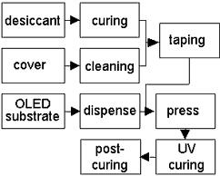
(2) Process and equipment development
The packaging process is shown in Figure 4. In order to place the Desiccant on the cover plate and smoothly bond the cover plate to the substrate, it needs to be carried out in a vacuum environment or the cavity is filled with an inert gas, such as nitrogen. It is worth noting that how to make the process of connecting the cover plate and the substrate more efficient, reduce the cost of the packaging process, and reduce the packaging time to achieve the best mass production rate, has become the three main goals of the development of packaging process and equipment technology.
Our other product:


