TFT: Thin film transistor
LCD: Liquid Crystal Display
TFT-LCD was invented in 1960 and after continuous improvement, it was successfully commercialized as a notebook computer panel in 1991, and has since entered the TFT-LCD generation.
1. TFT-LCD structure:
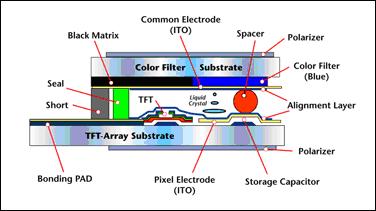
Simply put, the basic structure of a TFT-LCD panel is a layer of liquid crystal sandwiched between two glass substrates. Color filters are attached to the front LCD panel, and thin film transistors (TFT) are fabricated on the rear TFT panel. When a voltage is applied to the transistor, the liquid crystal turns and the light passes through the liquid crystal to produce a pixel on the front panel. The backlight module is located behind the TFT-Array panel and is responsible for providing light sources. Color filters give each pixel a specific color. Combining each pixel of different colors presents the image at the front of the panel.
1) TFT Pixel Element:
The TFT panel is composed of millions of TFT devices and ITO ((In TI Oxide, this material is a transparent conductive metal) area arranged like a matrix, and the so-called Array is the area of millions of neatly arranged TFT devices. , These millions of neatly arranged areas are the panel display area. The picture below shows the structure of a TFT pixel
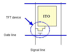
No matter how the design of the TFT board changes and how the manufacturing process is simplified, its structure must have a TFT device and a control liquid crystal area (if the light source is a transmissive LCD, the control liquid crystal area uses ITO, but for reflective LCD Use high-reflectivity metals, such as Al, etc.)
TFT device is a switch, its function is to control the number of electrons that flow into the ITO area. When the number of electrons flowing into the ITO area reaches the value we want, then turn off the TFT device, and at this time, the entire electrons are turned off ( Keep) in the ITO area.
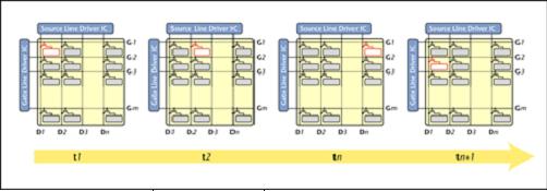
The above figure shows the time change specified for each pixel point. The gate driver IC continuously selects to turn on G1 from t1 to tn, so that the source driver IC charges the TFT pixels on G1 in the order of D1, D2 to Dn. At tn+1, the gate driver IC selects G2 again, and the source driver IC selects D1 in sequence.
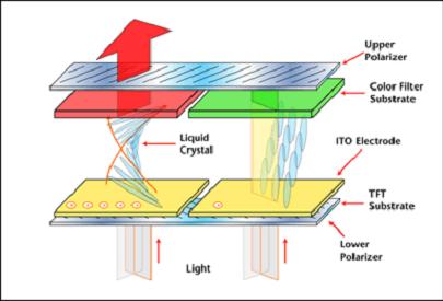
The above picture can express several things:
The more vertical the liquid crystal stands, the more light will not be guided by the liquid crystal. Different angles of the liquid crystal stand angle will guide different amounts of light. In the above example, the larger the liquid crystal stand angle, the more light it can penetrate. The weaker the light. (The direction in which the upper and lower polarizers are arranged will determine the strength of the transmitted light, so it is enough to understand the strength of the light guided by the angle at which the liquid crystal stands).
Unguided light will be absorbed by the upper polarizer. The light in nature has its polarity in any direction. The function of using a polarizer is to filter out most of the light that oscillates in different directions, and only let light in a certain direction pass.
2. New generation and size
What is the relationship between the glass substrate and the size of each generation?
Many people don't understand the differences between different generations of factories in the TFT-LCD industry, but the principle is quite simple. The main difference between different generations of plants is the size of the glass substrate, and the panel is a product cut from a large glass substrate. The new generation of the factory, the larger the glass substrate, so more panels can be cut to increase production capacity and reduce costs, or can produce larger size panels (such as LCD TV panels).
The TFT-LCD industry just emerged in Japan in the 1990s, when Japan designed and built a first-generation factory (referred to as G1) process. The glass substrate of the first generation plant is about 30 X 40 cm in size, which is approximately equivalent to a full-open magazine and can be made into a 15-inch panel. At the time, Daqi Technology (later merged with Lianyou Optoelectronics to form AUO Optoelectronics) entered the industry in 1996. At that time, the technology had advanced to the 3.5 generation factory (G3.5), and the glass substrate size was about 60 X 72 cm. Since its evolution, AUO has developed to the sixth-generation factory (G6) manufacturing process, and the size of the G6 glass substrate has reached 150 X 185 cm, which is equivalent to the size of a double bed. A piece of G6 glass substrate can cut 30 pieces of 15-inch panels. Compared with G3.5 which can cut 4 pieces and G1 can only make 1 piece of 15-inch panels, the production capacity of the sixth-generation factory is enlarged by multiples, and the relative cost is reduce. In addition, the huge size of the G6 glass substrate can also cut large-size panels, which can produce 8 32-inch LCD TV panels, which improves the diversification of panel product applications. Therefore, the global TFT-LCD manufacturers are all investing in the process technology of the new generation plant.
3. Introduction to TFT-LCD manufacturing process
1) What is TFT-LCD?
TFT-LCD is the abbreviation of thin-film transistor liquid-crystal display. How does TFT-LCD light up? Simply put, a TFT-LCD panel can be regarded as a layer of liquid crystal sandwiched between two glass substrates. The upper glass substrate is a color filter (Color Filter), while the lower glass is embedded with transistors. When the current passes through the transistor, the electric field changes, causing the liquid crystal molecules to deflect, thereby changing the polarization of the light, and then using the polarizer to determine the light and dark state of the pixel. In addition, the upper glass is laminated with the color filter, so that each pixel contains three colors of red, blue and green. These red, blue and green pixels form the image on the panel.
2) Three main manufacturing processes of TFT-LCD:
(1) Front Array
-The Array process in the previous stage is similar to the semiconductor process, but the difference is that thin film transistors are fabricated on glass instead of on silicon wafers.
(2) Middle Cell
-The cell in the middle section is the glass substrate of the previous Array, combined with the glass substrate of the color filter, and liquid crystal (LC) is poured between the two glass substrates.
(3) Module Assembly (Module Assembly)
-The back-end module assembly process is a production operation in which the glass after the Cell process is assembled with other components such as backlight boards, circuits, and outer frames.
4. The latest technology research and development
1) Organic light emitting display
Organic Light Emitting Display (Organic Light EmitTIng Display) or Organic Light Emitting Diode (Organic Light EmitTIng Diode), abbreviated as OLED, this technology has the following superior use characteristics.
l Self-luminous
l Ultra-thin characteristics
l High brightness
l High luminous efficiency
l High contrast
l Microsecond response time
l Ultra-wide viewing angle
l Low power consumption
l Large operating temperature range
l Flexible panel
l Low temperature polysilicon
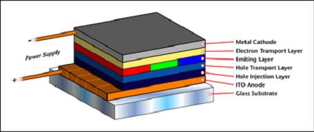
The principle of light emission is to vaporize an organic film between a transparent anode and a metal cathode, inject electrons and holes, and use them to recombine between the organic films to convert energy into visible light. And it can be matched with different organic materials to emit different colors of light to meet the needs of full-color displays.
2) Active OLED
Organic light-emitting displays can be divided into passive (Passive Matrix, PMOLED) and active (AcTIve Matrix, AMOLED) according to their driving methods. The so-called active drive OLED (AMOLED) uses Thin Film Transistor (TFT) and a capacitor to store signals to control the brightness and grayscale performance of the OLED.
Although the production cost and technical threshold of passive OLED are low, it is restricted by the driving method and the resolution cannot be improved. Therefore, the size of the application product is limited to about 5", and the product will be limited to the low-resolution and small-size market. If you want to get high Fine and large images must be driven in an active manner. The so-called active drive uses capacitors to store the signal, so the pixels can still maintain the original brightness after the scan line is scanned; as for the passive drive, only the scan line selects it. Pixels will be lit. Therefore, in the active driving mode, OLED does not need to be driven to a very high brightness, so it can achieve better life performance and high resolution requirements. OLED combined with TFT technology can be The realization of active driving of OLED can meet the requirements for the smoothness of picture playback and higher resolution in the current display market, and fully demonstrate the above-mentioned superior characteristics of OLED.
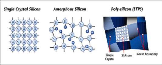
The technology for growing TFTs on glass substrates can be amorphous silicon (a-Si) and low temperature poly-silicon (LTPS) processes. The biggest difference between LTPS TFT and a-Si TFT lies in its The difference between electrical properties and the complexity of the manufacturing process. LTPS TFT has a higher carrier mobility, which means that the TFT can provide more sufficient current, but its manufacturing process is more complicated; while a-Si TFT is the opposite, although the carrier of a-Si The sub-movement rate is not as good as that of LTPS, but because its manufacturing process is simple and mature, it has a better competitive advantage in cost. Looking at the companies that develop active OLEDs in the world, only AUO has successfully combined OLED with LTPS and a-Si TFT at the same time, becoming the leader in active OLED technology.
3) Low temperature polysilicon
(1) What is LTPS?
Polysilicon (polysilicon) is a material with a size of about 0.1 to several um, based on silicon, composed of many silicon particles. In the semiconductor manufacturing industry, polysilicon is usually processed by LPCVD (Low Pressure Chemical Vapor Deposition) and then subjected to an annealing procedure higher than 900C. This method is called SPC (Solid Phase Crystallization). However, this method is not suitable for the flat-panel display manufacturing industry because the maximum temperature of glass is only 650C. Therefore, LTPS technology is especially applied to the manufacture of flat-panel displays.
(2) There are many methods to make LTPS film on glass or plastic substrate:
1. Metal Induced Crystallization (MIC): It is one of the SPC methods. However, compared to traditional SPC, this method can produce polysilicon at a lower temperature (about 500~600 C). This is because the thin layer of metal is coated before crystal formation, and the metal component plays an active function of reducing crystallization.
2. Cat-CVD: A method of directly depositing poly-film without vapor extraction. The deposition temperature can be lower than 300C. The growth mechanism includes the catalytic cracking reaction of the SiH4-H2 mixture.
3. Laser anneal: This is currently the most widely used method. Excimer laser is the main power used to heat and melt a-Si, which contains a low amount of hydrogen and then recrystallizes into poly-film.
There are many ways to make LTPS films on glass or plastic substrates:
The production of LTPS film is much more complicated than that of a-Si, but LTPS TFT is a hundred times more mobile than a-Si TFT. And can directly perform CMOS program on the glass substrate. Listed below are several characteristics of p-Si superior to a-Si:
1. The mobility of thin film transistors is faster, so the drive circuit can be made directly on the glass substrate, thus reducing the cost.
2. Vehicle for OLED: High mobility means that it can provide a larger drive current for OLED devices, so it is more suitable as a substrate for active OLED displays.
3. Compact modules: As part of the drive circuit can be made on the glass substrate, the circuit on the PCB is relatively simple, which can save the area of the PCB.
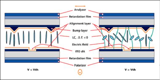
5. MVA
The MVA technology not only improves the viewing angle of the panel due to the special arrangement mode of the liquid crystal, but also solves most of the grayscale inversion problems.
The advantages of using MVA technology are:
l High contrast
l Wide viewing angle
l No grayscale inversion
l High resolution
l Fast response time
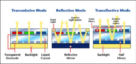
6. Semi-transmissive and semi-reflective
The LCD screen needs to show the image through the backlight through the color filter, and then it is reflected in our eye window. This backlight mode is called "transmissive". Most of the power of the LCD screen is consumed by the backlight device. . The brighter the backlight, the higher the brightness in front of the screen, but the more power it consumes.
The "reflective" structure uses an external light source to display the picture through a reflector plate. This device saves power but it is harder to see the picture when there is no external light source.
The "semi-transmissive and semi-reflective" type is a compromise between the two. This device uses a half mirror to replace the reflector. In addition to the backlight, it can also use the reflection of an external light source to save power, improve brightness and The effect of reducing weight.
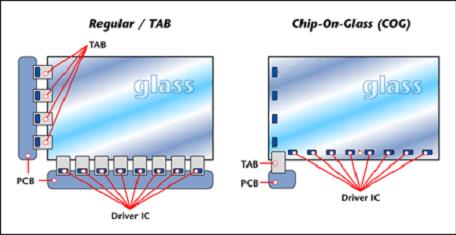
7. COG
Different from the traditional manufacturing process: COG technology assumes the driver IC directly on the glass substrate. The advantages of this technology include:
l Improve packaging density and reduce weight to make the panel lighter and thinner
l Reduce the use of materials and reduce production costs
l Improve panel resolution
8. ODF
The ODF process is an epoch-making manufacturing method. In the past, it was time-consuming, low-yield and difficult to achieve; such as the production of large-scale panel TV products, small Gap panels that respond to fast response, or advanced and high-quality MVA panels, using ODF process technology , The problem can be solved easily.
A simple comparison between the traditional process and the ODF process is as follows:
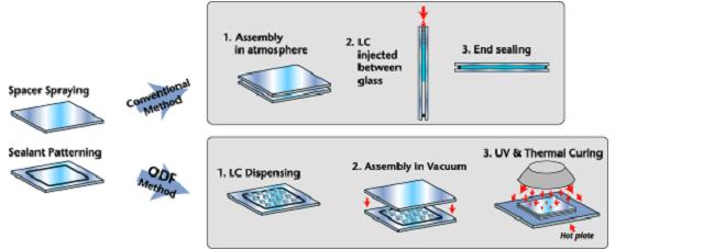
Using the ODF process, the advantages we can get from it are:
1. Decrease in machine investment: With ODF process, we no longer need vacuum tempering process, liquid crystal injection machine, sealing machine and panel cleaning equipment after sealing.
2. Space and manpower saving: Due to the reduction of the manufacturing process described in Project 1, the relative manpower and space can be saved.
3. Material saving: Generally speaking, in the ODF process, the use efficiency of the liquid crystal is more than 95%, but compared with the 60% of the traditional process, it can save more than 35% of the liquid crystal material cost. It can save the water, electricity, gas and lotion needed for the sealing glue and related panel cleaning.
4. Reduced manufacturing time: Because the saved process was originally the most time-consuming and time-consuming process in the traditional process, and with the large-scale trend of the panel, or the high-quality panel of the small cell gap, the time will be longer. Usually, the Cell process needs at least three days to complete in the traditional way, but for the ODF process, it can be completed in less than a day.


|
|
|
|
How far(long) the transmitter cover?
The transmission range depends on many factors. The true distance is based on the antenna installing height , antenna gain, using environment like building and other obstructions , sensitivity of the receiver, antenna of the receiver . Installing antenna more high and using in the countryside , the distance will much more far.
EXAMPLE 5W FM Transmitter use in the city and hometown:
I have a USA customer use 5W fm transmitter with GP antenna in his hometown ,and he test it with a car, it cover 10km(6.21mile).
I test the 5W fm transmitter with GP antenna in my hometown ,it cover about 2km(1.24mile).
I test the 5W fm transmitter with GP antenna in Guangzhou city ,it cover about only 300meter(984ft).
Below are the approximate range of different power FM Transmitters. ( The range is diameter )
0.1W ~ 5W FM Transmitter :100M ~1KM
5W ~15W FM Ttransmitter : 1KM ~ 3KM
15W ~ 80W FM Transmitter : 3KM ~10KM
80W ~500W FM Transmitter : 10KM ~30KM
500W ~1000W FM Transmitter : 30KM ~ 50KM
1KW ~ 2KW FM Transmitter : 50KM ~100KM
2KW ~5KW FM Transmitter : 100KM ~150KM
5KW ~10KW FM Transmitter : 150KM ~200KM
How to contact us for the transmitter?
Call me +8618078869184 OR
Email me [email protected]
1.How far you want to cover in diameter ?
2.How tall of you tower ?
3.Where are you from ?
And we will give you more professional advice.
About Us
FMUSER.ORG is a system integration company focusing on RF wireless transmission / studio video audio equipment / streaming and data processing .We are providing everything from advice and consultancy through rack integration to installation, commissioning and training.
We offer FM Transmitter, Analog TV Transmitter, Digital TV transmitter, VHF UHF Transmitter, Antennas, Coaxial Cable Connectors, STL, On Air Processing, Broadcast Products for the Studio, RF Signal Monitoring, RDS Encoders, Audio Processors and Remote Site Control Units, IPTV Products, Video / Audio Encoder / Decoder, designed to meet the needs of both large international broadcast networks and small private stations alike.
Our solution has FM Radio Station / Analog TV Station / Digital TV Station / Audio Video Studio Equipment / Studio Transmitter Link / Transmitter Telemetry System / Hotel TV System / IPTV Live Broadcasting / Streaming Live Broadcast / Video Conference / CATV Broadcasting system.
We are using advanced technology products for all the systems, because we know the high reliability and high performance are so important for the system and solution . At the same time we also have to make sure our products system with a very reasonable price.
We have customers of public and commercial broadcasters, telecom operators and regulation authorities , and we also offer solution and products to many hundreds of smaller, local and community broadcasters .
FMUSER.ORG has been exporting more than 15 years and have clients all over the world. With 13 years experience in this field ,we have a professional team to solve customer's all kinds of problems. We dedicated in supplying the extremely reasonable pricing of professional products & services. Contact email : [email protected]
Our Factory
We have modernization of the factory . You are welcome to visit our factory when you come to China.
At present , there are already 1095 customers around the world visited our Guangzhou Tianhe office . If you come to China , you are welcome to visit us .
At Fair
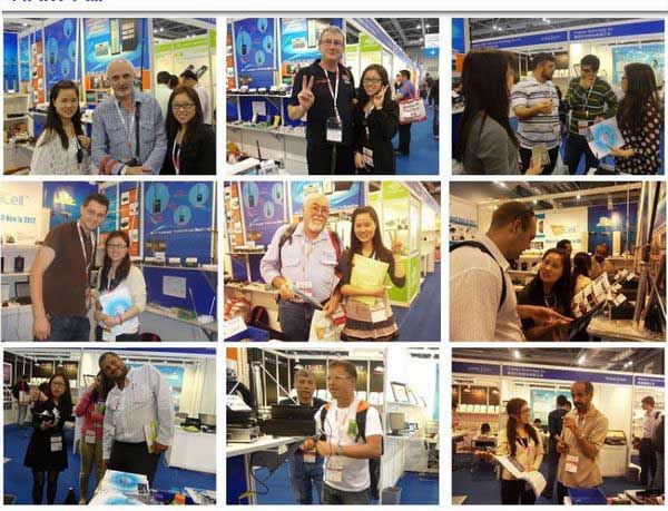
This is our participation in 2012 Global Sources Hong Kong Electronics Fair . Customers from all over the world finally have a chance to get together.
Where is Fmuser ?
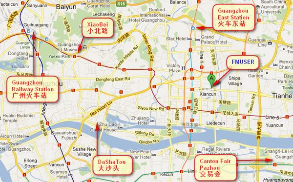
You can search this numbers " 23.127460034623816,113.33224654197693 " in google map , then you can find our fmuser office .
FMUSER Guangzhou office is in Tianhe District which is the center of the Canton . Very near to the Canton Fair , guangzhou railway station, xiaobei road and dashatou , only need 10 minutes if take TAXI . Welcome friends around the world to visit and negotiate .
Contact: Sky Blue
Cellphone: +8618078869184
WhatsApp: +8618078869184
Wechat: +8618078869184
E-mail: [email protected]
QQ: 727926717
Skype: sky198710021
Address: No.305 Room HuiLan Building No.273 Huanpu Road Guangzhou China Zip:510620
|
|
|
|
English: We accept all payments , such as PayPal, Credit Card, Western Union, Alipay, Money Bookers, T/T, LC, DP, DA, OA, Payoneer, If you have any question , please contact me [email protected] or WhatsApp +8618078869184
-
PayPal.  www.paypal.com www.paypal.com
We recommend you use Paypal to buy our items ,The Paypal is a secure way to buy on internet .
Every of our item list page bottom on top have a paypal logo to pay.
Credit Card.If you do not have paypal,but you have credit card,you also can click the Yellow PayPal button to pay with your credit card.
---------------------------------------------------------------------
But if you have not a credit card and not have a paypal account or difficult to got a paypal accout ,You can use the following:
Western Union.  www.westernunion.com www.westernunion.com
Pay by Western Union to me :
First name/Given name: Yingfeng
Last name/Surname/ Family name: Zhang
Full name: Yingfeng Zhang
Country: China
City: Guangzhou
|
---------------------------------------------------------------------
T/T . Pay by T/T (wire transfer/ Telegraphic Transfer/ Bank Transfer)
First BANK INFORMATION (COMPANY ACCOUNT):
SWIFT BIC: BKCHHKHHXXX
Bank name: BANK OF CHINA (HONG KONG) LIMITED, HONG KONG
Bank Address: BANK OF CHINA TOWER, 1 GARDEN ROAD, CENTRAL, HONG KONG
BANK CODE: 012
Account Name : FMUSER INTERNATIONAL GROUP LIMITED
Account NO. : 012-676-2-007855-0
---------------------------------------------------------------------
Second BANK INFORMATION (COMPANY ACCOUNT):
Beneficiary: Fmuser International Group Inc
Account Number: 44050158090900000337
Beneficiary's Bank: China Construction Bank Guangdong Branch
SWIFT Code: PCBCCNBJGDX
Address: NO.553 Tianhe Road, Guangzhou, Guangdong,Tianhe District, China
**Note: When you transfer money to our bank account, please DO NOT write anything in the remark area, otherwise we won't be able to receive the payment due to government policy on international trade business.
|
|
|
|
* It will be sent in 1-2 working days when payment clear.
* We will send it to your paypal address. If you want to change address, please send your correct address and phone number to my email [email protected]
* If the packages is below 2kg,we will be shipped via post airmail, it will take about 15-25days to your hand.
If the package is more than 2kg,we will ship via EMS , DHL , UPS, Fedex fast express delivery,it will take about 7~15days to your hand.
If the package more than 100kg , we will send via DHL or air freight. It will take about 3~7days to your hand.
All the packages are form China guangzhou.
* Package will be sent as a "gift" and declear as less as possible,buyer don't need to pay for "TAX".
* After ship, we will send you an E-mail and give you the tracking number.
|
|
|
For Warranty .
Contact US--->>Return the item to us--->>Receive and send another replace .
Name: Liu xiaoxia
Address: 305Fang HuiLanGe HuangPuDaDaoXi 273Hao TianHeQu Guangzhou China.
ZIP:510620
Phone: +8618078869184
Please return to this address and write your paypal address,name,problem on note: |
|