What this design is for
To boost the output power of low power FM broadcast band exciters, a number of these are available commercially, both as kits and ready made. See How to be a Community Radio Station for links to reviews of some of the more popular exciters.
Who is this design for?
- Those who are familiar with the RF electronics and mechanical constructional techniques
- Those who have already successfully constructed and tested VHF power (> 10W) amplifiers
For reference, see Introduction to Community Radio Station Electronics
The following test equipment will be required to tune the amplifier:
- Stabilised current limited power supply (+28V, 3A)
- Multimeter, with 3A or greater current range
- 50W VHF Dummy Load
- RF Power Meter
- FM exciter, with approx. 26 - 27 dBm output power
- RF Spectrum Analyser
- RF Network Analyser or a spectrum analyser with tracking generator
- RF power attenuator
This design is NOT suitable for beginners and VHF RF novices. These people run the following risks:
- Thermal and RF burns
- Electrocution
- Destruction of expensive RF components and test equipment
- Unwanted spurious RF radiation, resulting in interference to other users of the electromagnetic spectrum, thus risking a visit from the state, and consequent risk of equipment confiscation, fines, and possibly imprisonment.
- A great deal of stress and frustration.
Why this design is necessary
I believe the quality of the vast majority of schematics and designs for FM broadcast equipment available on the internet to be far from satisfactorily. See my advice on building from plans on the web. In particular the information available on VHF RF power amplifiers is even more desperate, for example designs using dinosaurs of devices such as the TP9380. This design is based on a new MOSFET device, with the attendant advantages of
- high gain
- high efficiency
- ease of tuning
Seeing as most of the designs on the web are over 10 years old, using a recently introduced device should maximise the useful life of the design. I also use this design as a vehicle to demonstrate the amount of information required for a third party not equipped with mind-reading skills to successfully build this amplifier. The point is this: if a person is sufficiently skilled and experienced to build something from scanty design information, for instance just a schematic, they are just as able to build it from no information at all. Conversely, a person not at that skill and experience level will require detailed instructions to succeed.
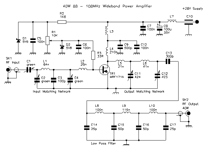
The amplifier design is based on the recently introduced (1998) Motorola MRF171A MOSFET (MRF171A data sheet in PDF format).Do not confuse this with the older, now discontinued, MRF171 device. January 2002 - Motorola changes their RF power device product portfolio more oftern than some people change their underparts. It looks like Motorola have unloaded this device on to M/A-Com.
Computer Simulation
The initial feasibility was performed using a linear RF and microwave simulation package, specifically Supercompact. The version used was 6.0, which quite frankly I consider a piss-poor piece of software and don't recommend at all. For this device, Motorola provide S parameters and large signal single ended impedances. The S parameters are measured at 0.5 A quiescent drain current, which represents a step forward in device characterisation, as traditionally S parameters tended to be measured at quite low drain currents. Whilst this is satisfactory for small-signal devices, the use of S parameters measured at small drain currents is limited for power amplifier design.
While the S parameter information measured at 0.5 A could have provided a useful design starting point, I choose to base the design on the single ended large-signal impedances. These are measured by the device manufacturer by tuning the device up for best performance at each test frequency in a generic test fixture. The test device is then removed, and a vector network analyser is used to measure the complex impedance looking back into the matching network, whilst these are terminated with 50 R. This procedure is carried out for the input and output matching networks. The advantage of large signal impedance data is that it can be measured at the actual output power that the device is designed to generate, and as such are more representative in a power amplifier scenario. Note the large-single impedances only provide information to enable an input and output matching network to be synthesised, they provide no information about the likely gain, efficiency, noise performance (if relevant) or stability of the resulting amplifier.
This is the file used to synthesise the input network.
* mrf171i1.ckt ;Name of file
* variable definition block, first value is minimum allowed value,
* third is maximum allowed value, middle is variable
C1: ? 1PF 30.2596PF 120PF ?
C2: ? 1PF 21.8507PF 120PF ?
L1: ? 1NH 72.7228NH 80NH ?
C3: ? 1PF 179.765PF 180PF ?
L2: ? 1NH 30.4466NH 80NH ?

BLK				;Circuit netlist

   cap 1 2 c=c1
   cap 2 0 c=c2
   ind 2 3 l=l1
   cap 3 0 c=c3
   ind 3 9 l=l2
   res 9 0 r=33			;gate bias feed resistor
   one 9 mrf171ip		;reference to 1 port data

   IPNET: 1POR 1		;create a new 1 port network

END

FREQ
   STEP 88MHZ 108MHZ 1MHZ
END

OPT
* Optimisation control statement, tells simulator to optimise between
* 88 and 108 MHz, and to achieve a input return loss of better than
* -24 dB
   IPNET  R1 = 50
   F = 88MHZ 108MHZ
   MS11 -24DB LT
END

DATA
* Define a one port network called mrf171ip, referencing the large-signal
* series equivalent complex impedances.  This data is available at 4
* frequency points
* Define Z parameter information, real and imaginary format,
* reference impedance is 1 Ohm
   mrf171ip: Z RI RREF=1
   * MRF171A Z SOURCE

   30MHZ	12.8	-3.6
   100MHZ	3.1 	-11.6
   150MHZ	2.0 	-6.5
   200MHZ	2.2 	-6.0

END
Of course, the use of a simulator doesn't provide any assistance in the selection of circuit topology, nor the starting values for the network components. This information comes from design experience. All optimisation values have been constrained with maxima and minima to keep the resulting network realisable.
Initially, a 3 pole matching network was tried, this was not capable of providing a sufficiently broadband match across the 20 MHz. Using a 5 pole circuit allowed the optimisation goal to be achieved. Note the 33R gate bias is included in the simulation, as this helps de-Q the input network, and improves the stability in the final amplifier.
A similar procedure was performed for the output network. In this simulation, the drain feed was included in the simulation. Although on the face of it, the value of this choke is not critical, if it gets too large stability can be comprised, if it gets too small, it becomes part of the output matching network, which in this case was thought not be desirable.
Component choices
As the input power is only half a watt, standard ceramic capacitors and trimmers were used in the input matching circuit. L1 and L2 (refer to schematic) could have been made much smaller, but were kept big for consistency with the inductors used in the output network. On the output network, mica metal clad capacitors and mica compression trimmers were used to handle the power and keep component losses to a minimum. The wideband choke L3 provides some lossy reactance at lower RF frequencies, C8 takes care of AF (audio frequency) decoupling.
The use of an enhancement mode N-channel MOSFET (a positive voltage biases the device into conduction) means the bias circuitry is simple. A potential divider taps off the required voltage from a low voltage stabilised by a 5.6V zener diode. The second 5.6V zener, D2, is fitted as a precautionary measure to ensure excessive voltage are not applied to the gate of the FET, this would certainly result in the destruction of the device. Purists would temperature stabilise the bias current, but as the bias is not critical in this application, this was not bothered with.
A BNC socket had been used for the RF input, due to the low RF input power. I've used N type for the RF output, I don't use BNC for above about 5W and I don't like UHF style connectors. Personally, I don't recommend using UHF connectors above 30MHz.
The amplifier was constructed in a small aluminium diecast box. RF input and output connections are made by coaxial sockets. The power supply is routed through a ceramic feedthrough capacitor bolted in the wall of the box. This constructional techniques results in excellent shielding, preventing RF radiation escaping from the amplifier. Without it, significant amounts of RF radiation could be radiated, interfering with other sensitive circuits such as VCOs and audio stages, also significant amounts of harmonic radiation could occur.
The base of the power device sits through a cut-out in the floor of the diecast box and is bolted directly onto a small extruded aluminium heatsink. An alternative would have the base of the power device sitting on the floor of the diecast box. This is not recommended for two reasons, both concerned with providing an effective path to conduct heat from the FET. Firstly the floor of the diecast box is not particularly smooth, which results in a poor thermal path. Secondly, having the floor of the diecast box in the thermal path introduces more mechanical interfaces and hence more thermal resistance. Another advantage of the chosen constructional technique is that it correctly aligns the device leads with the top face of the circuit board.
Using the specified heatsink will require the use of forced air cooling (a fan). If you plan not to use a fan, a much bigger heatsink will be required, and the amplifier should be mounted with the heatsink fins vertical to maximise cooling by natural convection.
The circuit board consists of a piece of fibre glass PCB (printed circuit board) material clad with 1oz Cu (copper) each side. I used Wainwright to form the circuit nodes - this is basically self-adhesive bits of tinned single sided PCB material, cut to size with a hefty pair of side-cutters. An easy alternative is to use pieces of 1.6mm thick single sided PCB material, cut to size and then tinned. These are glued onto the ground plane with a cyanoacrylate type adhesive (e.g super-glue or Tak-pak FEC 537-044). This method of construction results in the top side of the PCB being an excellent ground plane. The only exception to this are the two pads for the gate and drain of the FET. These were created by carefully scoring the top layer of copper with a sharp scalpel, and then removing the slivers of copper with the assistance of a fine point soldering iron tip and the scalpel. Running the iron tip along the isolated piece of copper loosens the glue sufficiently for the Cu to be peeled off with the scalpel. The gate pad thus created is clearly visible in the photograph of the prototype
Having made the aperture in the PCB for the base of the power device to sit through, I wrapped copper tape through the slot to join the upper and lower ground planes. This was done in two places, underneath the source tabs. The copper tape was then soldered top and bottom.
See photograph for suggested component positions. The vertical screen to the right of the enclosure is a piece of double sided PCB material, soldered to the top ground plane on both sides. This is an attempt to improve the final harmonic rejection, by reducing coupling between the inductors that form the output match and the inductors making up the LPF. To do these kind of soldering jobs a 60W or greater soldering iron will be required - preferably a temperature controlled one. This iron will be too over the top for the smaller components so a smaller iron will be required as well.
As mentioned below, the LPF inductors are soldered directly to the tabs of the metal clad capacitors.
Suggested Rough and Ready Construction Procedure
- Cut out a piece of double sided PCB material for the main board (approx. 100 x 85mm)
- Create the aperture for the FET, using a selection of drills and files. Use the FET as a template, if required, but don't blow it up with static. Make sure you'll end up with the drain on the right side.
- Drill six holes in the PCB, these are to hold the PCB to the diecast box
- Place the PCB in the box and use the holes in the PCB to drill through the box
- Temporarily screw the PCB to the box
- Work out where the heatsink is going to go, underneath the box The device should end up towards the centre of the heatsink. Either drill some more holes through the whole lot, and re-use some of the existing PCB/box holes and extend these down through the heatsink. Temporarily screw the heatsink to the PCB/box assembly. When you look into the top of the box you should now see a piece of heatsink revealed, the same size as the base of the FET.
- Rig yourself up some static protection (if you've got an old blown-up device or a bipolar device in the same package you won't have to bother with this) and drop the device into the aperture in the board.
- Use the FET to give you give the centre positions of its' mounting holes
- Take everything to bits again. Make two holes in the heatsink for the FET
- Drill the holes in the two ends of the box for the RF connectors and the feedthrough capacitor
- Tin the PCB, top and bottom, with a big iron. Use just enough solder to get a smooth finish but not too much to create raised areas of solder, especially on the bottom, as these will prevent the PCB sitting flat against the box floor.
- Create the two islands for the FET gate and drain, as detailed in the above paragraph
- Solder copper tape between top and bottom faces of the PCB underneath where the source tabs will be
- Create the PCB islands, tin them, stick them on the PCB using the photograph as a guide
- Create and fit the screen between the amplifier and the LPF areas
- Fit all the remaining PCB components, with the exception of the FET
- Fit the PCB to the box and the heatsink
- Fit the and connect and the RF connectors and the feed-through capacitor
- Taking anti-static precautions again, apply the thinnest continuous film possible of heat transfer paste to the base of the FET. This can be conveniently done with a wooden cocktail stick
- Bend up the last 2mm of each of the FET's leads. This will make it much easier to remove, should the need arise
- Screw the FET to the heatsink. Too loose and the device will over-heat, too tight and you will distort the flange of the device and once again it will overheat. If you've got a torque screwdriver, look up the recommended torque and use it.
- If you've understood the instructions correctly, the tabs of the device will be fractionally above the PCB Solder the FET in with the big iron, first the sources, then the drain, finally the gate. You may have to disconnect L4 and L5 while you are fitting the FET, but don't disconnect R3 as this provides static protection for the device.
| Reference |
Description |
FEC Part No. |
Quantity |
| C1, C2, C4 |
5.5 - 50p miniature ceramic trimmer (green) |
148-161 |
3 |
| C3 |
100p ceramic disc 50V NP0 dielectric |
896-457 |
1 |
| C5, C6, C7 |
100n multilayer ceramic 50V X7R dielectric |
146-227 |
3 |
| C8 |
100u 35V electrolytic radial capacitor |
667-419 |
1 |
| C9 |
500p metal clad capacitor 500V |
|
1 |
| C10 |
1n ceramic lead through capacitor capacitor |
149-150 |
1 |
| C11 |
16 - 100p mica compression trimmer capacitor (Arco 424) |
|
1 |
| C12 |
25 - 150p mica compression trimmer capacitor (Arco 423 or Sprague GMA30300) |
|
1 |
| C13 |
300p metal clad capacitor 500V |
|
1 |
| C14, C17 |
25p metal clad capacitor 500V |
|
2 |
| C15, C16 |
50p metal clad capacitor 500V |
|
2 |
| L1 |
64nH inductor - 4 turns 18 SWG tinned Cu wire on 6.5mm dia. former, turns length 8mm |
|
1 |
| L2 |
25nH inductor - 2 turns 18 SWG tinned Cu wire on 6.5mm dia. former, turns length 4mm |
|
1 |
| L3 |
6 hole ferrite bead threaded with 2.5 turns 22 SWG tinned Cu Wire to form wideband choke |
219-850 |
1 |
| L4 |
210nH inductor - 8 turns 18 SWG enamelled Cu wire on 6.5mm dia. former, turns length 12mm |
|
1 |
| L5 |
21nH inductor - 3 turns 18 SWG tinned Cu wire on 4mm dia. former, turns length 10mm |
|
1 |
| L6 |
41nH inductor - 4 turns 22 SWG tinned Cu wire on 4mm dia. former, turns length 6mm |
|
1 |
| L7 |
2 ferrite beads threaded onto lead of C10 |
242-500 |
2 |
| L8, L10 |
100nH inductor - 5 turns 18 SWG tinned Cu wire on 6.5mm dia. former, turns length 8mm |
|
2 |
| L9 |
115nH inductor - 6 turns 18 SWG tinned Cu wire on 6.5mm dia. former, turns length 12mm |
|
1 |
| R1 |
10K cermet potentiometer 0.5W |
108-566 |
1 |
| R2 |
1K8 metal film resistor 0.5W |
333-864 |
1 |
| R3 |
33R metal film resistor 0.5W |
333-440 |
1 |
| D1, D2 |
BZX79C5V6 400mW Zener Diode |
931-779 |
2 |
| TR1 |
MRF171A (Motorola) |
|
1 |
| SK1 |
BNC bulkhead socket |
583-509 |
1 |
| SK2 |
N type panel socket, square flange |
310-025 |
1 |
| |
|
|
|
| |
Diecast Box 29830PSL 38 x 120 x 95mm |
301-530 |
1 |
| |
Heatsink 16 x 60 x 89mm 3.4°C/W (Redpoint Thermalloy 3.5Y1) |
170-088 |
1 |
| |
Double sided Cu clad PCB material 1.6mm thick |
|
A/R |
| |
Copper Tape or Foil |
152-659 |
A/R |
| |
M3 nut, bolt, crinkly washer set |
|
16 |
| |
Non-Silicone Heat Transfer Paste |
317-950 |
A/R |
Notes
- Farnell Part Numbers are for guide only - other equivalent parts can be substituted.
- Metal clad capacitors are either Semco MCM series, Unelco J101 series, Underwood, or Arco MCJ-101 series available from, amongst other places, RF Parts.
- MRF171A available from BFI (UK), Richardson or RF Parts (US)
- Arco or Sprague trimmers are available from Communication Concepts (US)
- 18 SWG (standard wire gauge) is approximately 1.2mm diameter
- 22 SWG (standard wire gauge) is approximately 0.7mm diameter
- To make the inductors - wind the required number of turns round an appropriately sized former, initially use one wire diameter spacing between each turn. Then pull the turns apart to get the length required in the parts list table. Finally check the value using a network analyser and adjust accordingly.
- The exception to the above spacing rule is L4, which is close wound.
- Copper foil is available from craft shops (used in stained glass making)
- A/R = as required
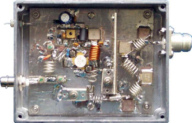
Note orientation of the FET. The lead with the slash is the drain, and is to the right
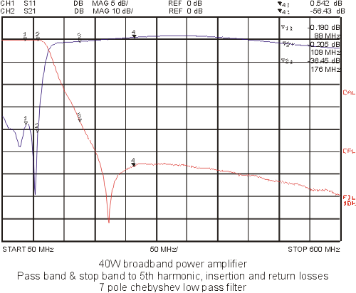
Any RF power amplifier must be followed by a low pass filter (LPF) to reduce the harmonics to an acceptable level. What this level is in a unlicensed application is a moot point, but as the output power is increased, more attention must be be paid to the harmonic suppression. For example, a 3rd harmonic of -30dBc on a 1W unit is 1uW, which is unlikely to cause any bother, whilst -30dBc 3rd harmonic suppression on a 1KW output results in a 1W of power at the third harmonic which is potentially problematic. So for the absolute level of harmonic radiation in the second example to be the same as the first, we now need to suppress the third harmonic by 60dBc.
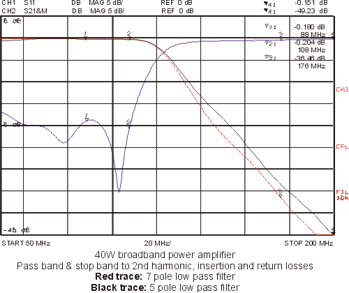
In this design I made the decision to implement a 7 pole Chebyshev low pass filter. A Chebyshev was chosen as the phase and amplitude ripple within the passband was not critical, and the Chebyshev gives a better stop band attenuation than compared to say, a Butterworth. The design stopband was chosen to 113MHz, giving a 5MHz implementation margin from the highest desired passband frequency at 108MHz and the start of the stopband at 113MHz. The next critical design parameter was the passband ripple. For a single frequency design it is normal practice to choose a large passband ripple, for example 1dB, and tune the peak of the last passband maxima to the desired output frequency. This gives the best stopband attenuation because greater passband ripple results in more rapid stopband attenuation. A seven pole filter has 7 reactive elements, in this design four capacitors and three inductors. The more poles, the better the stopband attenuation, at the expense of increased complexity and more passband insertion loss. An odd number of poles is required as both the input and output impedance was designed to be 50R.
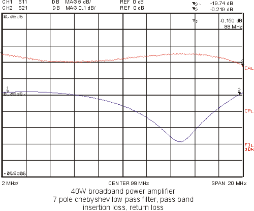
As this design is wideband, this constrains the passband ripple to a level such that the passband return loss does not become to horrible. Using the excellent Faisyn shareware filter design utility (available from FaiSyn RF Design Software Home Page) allows these trade-offs to be easily investigated, and I settled for a passband ripple of 0.02dB. This program also calculates the filter values for you, and outputs a netlist in a format suitable for inputting into the most popular linear circuit simulators. With 7 poles, the choice was available to use 4 capacitors and 3 inductors or 3 capacitors and 4 inductors. I chose the former, on the grounds that it results in one less component to wind. The capacitor values given from the faisyn program were examined to check that they were close to a preferred value, which they were. If they had fallen between preferred values, the options would include paralleling two capacitors together, which unnecessarily ups the component count, or subtly tweaking the stopband frequency and passband ripple to get a more desirable set of values.
To implement the filter, I decided to use standard size metal clad capacitors made by Unelco or Semco. The inductors were made from 18 SWG (standard wire gauge) tinned copper wire. In my experience there is little to be gained from using silver plated copper wire. The inductors were formed round of the centre of a standard RS or Farnell tweaking tool (FEC 145-507) - this has a diameter of 0.25 inch, 6.35mm. Otherwise use the appropriately sized drill bit. The outer two inductors were wound clockwise, the inner one was wound counter-clockwise. This is an attempt to reduce the mutual inductive coupling between the inductors, this tending to degrade the stopband attenuation. For the same reason the inductors are arranged at 90° to each other, rather than all in a straight line. The inductors are soldered directly to the tabs of the metal clad capacitors. This keeps losses to a minimum. A carefully constructed filter of this type can exhibit a passband insertion loss of better than 0.2dB. Here are the test results for the prototype unit.
Knowing the required values for the inductors, I made an educated guess based on experience as to how many turns I required, and then used a properly calibrated RF network analyser to measure the inductance of the inductor I had created. This is by far the most accurate way to determine the value of small value inductances, as the measurement can be made at the actual operating frequency of the filter. Having measured the value and adjusted the inductances accordingly, you should find that when the complete filter is constructed, surprisingly little adjustment is necessary to finalise the filter tuning.
The best way to tune this filter is to minimise the passband input return loss, using a network analyser. By minimising the input return loss you will minimise the passband transmission loss and passband ripple. The 20MHz span graph shows that I achieved a passband return loss of -18dB. If you don't have a network analyser, things are a bit trickier. If you just tuning up for a spot frequency, set up an RF power source to drive into the filter via a directional power meter. The filter is terminated with a good 50R load. Now monitor the reflected power coming back from the filter and tune the filter to minimise the reflected power. If you want wideband performance, you will have to try and do this at say, three frequencies, bottom, middle and top of the band. Alternatively, if you managed to measure you inductors well enough by other means, you could just assemble the filter and leave it at that, with no further adjustment.
Having tuned for minimum passband return loss, the stopband attenuation takes care of itself, you shouldn't tune for it as you will mess up the passband insertion loss. The 200MHz span graph shows I managed 36dB of rejection at the 2nd harmonic of 88MHz, which is the worst case. Referring to the 600MHz span graph shows the 3rd harmonic of 88MHz suppressed by -55dB, and the higher orders by an amount greater than this.
I used a HP 8714C network analyser to tune this amplifier. Without access to a network analyser, you are have to going to be extremely inventive to tune for wideband performance. Having tuned the LPF, the next job is to set the FET bias. Do this with a spectrum analyser connected to the output (via an appropriate amount of attenuation, at least 40dB) to monitor for spurious oscillations. Connect a good 50R load to the input and connect a stabilised PSU (power supply unit) with a current limit set to 200mA.
|
Note: This amplifier will oscillate (non-destructively) if it is powered up with no RF input connected, or if any RF stages preceding the amplifier are not powered up.
|
Set all trimmers to centre of their range. With the miniature ceramic trimmers specified, when the half moon metallisation on the top plate of the trimmer is fully aligned with the flat on the trimmer body, the trimmer is at maximum capacitance. Rotate 180° from here for minimum capacitance. Set R1 for minimum voltage (experiment before you fit the FET if you don't know which way this is). Slowly increase the supply voltage from 0V up to +28V. The only current drawn should be that taken by the bias circuit, about 14mA. Now adjust R1 to add 100mA to that figure. There should be no sudden steps in the current taken from the PSU. If there are, the amplifier is almost certainly oscillating.
If all is well, switch off. Calibrate the network analyser. On the HP 8714C for this application I normalise S11 into a open circuit and do a through calibration on S21 with 40dB of attenuation in line. Obviously the attenuators used must be rated for at least 50W of RF at VHF frequencies.
Now life gets slightly complicated. Normally I'd recommend looking through the amplifier and LPF combination, but because the LPF break point is only 5MHz above the desired passband of the amplifier, it makes it impossible to see the response shape of the amplifier if this happens to be upband from 108MHz. For this reason I did the initial amplifier tuning with the LPF bypassed, which allowed me to set the network analyser span wide enough to see where the amplifier response was.
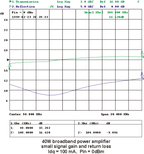
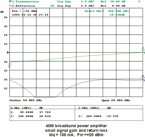
With 0dBm of drive, tweak away to get approximately 15dB of gain and better than 10dB of return loss across 88 to 108 MHz (small signal gain plot, Pin = 0 dBm). Now up the drive to the amplifier, backing off the current limit appropriately. You'll notice that as you increase the RF drive, the gain will increase and the input return loss will improve. This behaviour is a consequence of biasing the FET comparatively lightly. You could bias the nuts out of the FET, and bias it at, say 0.5A, this will give you more gain at lower drive levels. For normal applications I recommend using a lower bias. A high bias at small output levels will reduce the DC to RF efficiency.
You will now need to fan cool the amplifier, unless you have fitted it with an enormous heatsink. With the HP 8714C you can get +20dBm source power (that's what it says on the screen, it's actually less than that) (medium signal gain plot, Pin = +20 dBm). With this level of drive you can now tune for 18 to 20dB of gain and return loss better than 15dB. At this point I'd reconnect the LPF and narrow the network analyser span to 20MHz centred on 98MHz. Driving the amplifier above 108MHz at power into the LPF is certainly not recommended. Before you get too carried away switch to CW (best to lengthen the sweep sweep to several seconds on CW to avoid being confused by the analysers sweep fly-back) and have a look at the output on the spectrum analyser. The output should be clean as the driven snow, do remember to check the output is at at the frequency you're exciting the amplifier with, if it isn't you will be looking at an horrendous in-band oscillation.
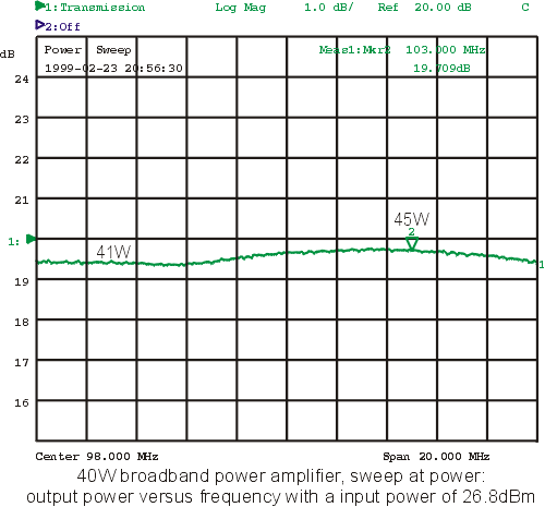
For the final power flatness tuning, because I had access to a smart RF laboratory with everything you could possibly require (test equipment wise, anyway) I used a Mini-Circuits ZHL-42W wideband amplifier to boost the output of the network analyser to enable me to tune the amplifiers' gain response flat at full output power. The final gain plot was taken by setting the source power appropriately, and then doing a through calibration with the Mini-Circuits amplifier and the power attenuators in-line. This allowed me to plot just the gain of the power amplifier. I then switched to slow sweep and used a calibrated RF power meter to accurately measure the RF output power. Knowing the RF output power and gain accurately allowed me to calculate the input power to the power amplifier. This plot shows the power gain is a shade under 20dB and about 0.3dB flat across the band (large signal gain plot, Pin = +26.8 dBm). In conjunction with the flatness tuning, the efficiency should be checked. I managed a minimum of 60% at 88MHz at 40W out, improving with higher output powers. I would say that good efficiency is more important than good flatness. From the listeners point of view, the difference between 35W and 45W output is negligible, but running a lower power with a good efficiency means the FET will run cooler, last longer and be more resilient to fault conditions like a high VSWR.
What output power you choose to finally run is up to you, the MRF171A will happily run at least 45W and probably a lot more, though I don't recommend it. Around 40 to 45W is plenty - see How to Keep your Final RF Power Device Alive for more information.
Amplifier Results
No harmonics could be measured at the output of the amplifier down to a noise floor of -70dBc. This is to be expected, as a quick investigation showed the raw harmonics of the amplifier before the LPF to about -40dBc. The filter has already been demonstrated to have a minimum 2nd harmonic suppression of -35dBc. No spurious output were visible.
No formal measurements were made with bad output VSWRs. I did accidentally run the amplifier at full power into an open circuit for a few seconds, and it didn't blow up. Using a PSU with a carefully set current limit will help prevent the amplifier doing anything stupid under these conditions.
As an example of an application for this amplifier I used the Broadcast Warehouse 1W FM LCD PLL Exciter to drive the 40W broadband amplifier. To avoid modifying the Broadcast Warehouse unit, I used a laboratory 3dB BNC pad between the exciter and the power amplifier, to provide the right drive level to the amplifier. The exciter was programmed for three different frequencies, at each frequency the output power and current consumption measured, allowing the DC to RF efficiency to be calculated.
Power Amplifier supply voltage = 28V
Exciter supply voltage = 14.0V, Exciter current consumption = 200 mA approx.
Frequency
(MHz) |
Current Consumption
(A) |
Pout
(W) |
DC to RF efficiency
(%) |
| 87.5 |
2.61 |
48 |
66 |
| 98.0 |
2.44 |
50 |
73 |
| 108.0 |
2.10 |
47 |
76 |
The Broadcast Warehouse exciter incorporates an out of lock RF shutdown facility, used during PLL reprogramming so that RF is not generated until frequency lock has been regained. When the exciters' RF shutdown was active, the amplifier output was similarly reduced - i.e. the amplifier remained stable.
I have demonstrated a wideband amplifier, that once tuned, requires no further adjustment to cover the 87.5 to 108MHz FM broadcast band. The design uses a state-of-the-art MOSFET providing nearly 20dB of gain with a single stage, has good DC to RF efficiency, low component count, and is simple to build. The parts cost should not exceed £50, the FET used in the prototype cost less than £25
If this amplifier is used with a broadband exciter and aerial, the resulting combination allows the user to switch transmitting frequency at will with no adjustments necessary anyway in the transmit chain.
The amplifier requires a fair degree of RF power experience to tune, and access to professional RF test equipment
- Build additional units to assess repeatability
- Design printed circuit board
- Improve stability under bad input mismatch conditions
- Reduce variable component count
- Investigate varying FET bias current to modify amplifier gain
Contributed
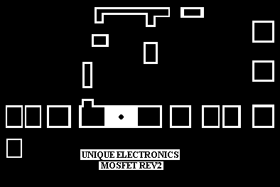
 Contributed by Unique Electronics (Woody and Alpy)
"Here's a PCB for the MRF171A, 45 watt mosfet, on your page.
The file is in bmp format. Use laser film and a laser printer, it will print to size."
MRF171A_1_colour.bmp (14 kb)
Our other product: