Do you want to DIY make a 5w fm transmitter yourself ? Come with me, get our 5w fm transmitter PCB kit suite to DIY the 5w fm transmitter, click here
At last!- a stereo FM transmitter that's a snack to align.
This new stereo FM Micromitter is capable of broadcasting good quality signals over a range of about 20 metres. It's ideal for broadcasting music from a CD player or from any other source so that it can be picked up in another location.
For example, if you don't have a CD player in you car, you can use the Micromitter to broadcast signals from a portable CD player to your car's radio. Alternatively, you might want to use the Micromitter to broadcast signals from your lounge-room CD player to an FM receiver located in another part of the house or by the pool.
Because it's based on a single IC, this unit is a snack to build and fits easily into a small plastic utility box. It broadcasts on the FM band (ie, 88-108MHz) so that its signal can be received on any standard FM tuner or portable radio.
However, unlike previous FM transmitters published in SILICON CHIP, this new design is not continuously variable over the FM broadcast band. Instead, a 4-way DIP switch is used to select one of 14 preset frequencies. These are available in two ranges covering from 87.7-88.9MHz and 106.7-107.9MHz in 0.2MHz steps.
Do you want to DIY make a 5w fm transmitter yourself ? Come with me, get our 5w fm transmitter PCB kit suite to DIY the 5w fm transmitter, click here
No tuning coils

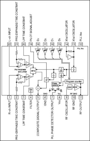
Fig.1: block diagram of the Rohm BH1417F stereo FM transmitter IC. The text explains how it works.
We first published an FM stereo transmitter in SILICON CHIP in October 1988 and followed this up with a new version in April 2001. Dubbed the Minimitter, these earlier versions were based on the popular Rohm BA1404 IC which is not being produced any more.
On both these earlier units, the alignment procedure requires careful adjustment of the ferrite tuning slugs within two coils (an oscillator coil and a filter coil), so that the RF output matched the frequency selected on the FM receiver. However, some constructors had difficulty with this because the adjustment was quite sensitive.
In particular, if you had a digital (ie, synthesised) FM receiver, you had to set the receiver to a particular frequency and then carefully tune the transmitter frequency "through" it. In addition, there was some interaction between the oscillator and filter coil adjustments and this confused some people.
That problem doesn't exist on this new design, since there is no frequency alignment procedure. Instead, all you have to do is set the transmitter frequency using the 4-way DIP switch and then dial-up the programmed frequency on your FM tuner.
After that, it's just a matter of adjusting a single coil when setting up the transmitter, to set for correct RF operation.
Improved specifications
The new FM Stereo Micromitter is now crystal-locked which means that the unit does not drift off frequency over time. In addition, the distortion, stereo separation, signal-to-noise ratio and stereo locking are much improved on this new unit compared to the earlier designs. The specifications panel has further details.
BH1417F transmitter IC
Do you want to DIY make a 5w fm transmitter yourself ? Come with me, get our 5w fm transmitter PCB kit suite to DIY the 5w fm transmitter, click here

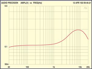
Fig.2: this frequency versus output level plot shows the composite level (pin 5). The 50ms pre-emphasis at around 3kHz causes the rise in response, while the 15kHz low pass roll off produces the fall in response above 10kHz.
At the heart of the new design is the BH1417F FM stereo transmitter IC made by the Rhom Corporation. As already mentioned, it replaces the now hard to find BA1404 that has been used in the previous designs.
Do you want to DIY make a 5w fm transmitter yourself ? Come with me, get our 5w fm transmitter PCB kit suite to DIY the 5w fm transmitter, click here
Fig.1 shows the internal features of the BH1417F. It includes all the processing circuitry required for stereo FM transmission and also the crystal control section which provides precise frequency locking.
As shown, the BH1417F includes two separate audio processing sections, for the left and right channels. The left-channel audio signal is applied to pin 22 of the chip, while the right channel signal is applied to pin 1. These audio signals are then applied to a pre-emphasis circuit which boosts those frequencies above a 50ms time constant (ie, those frequencies above 3.183kHz) prior to transmission.
Basically, pre-emphasis is used to improve the signal-to-noise ratio of the received FM signal. It works by using a complementary de-emphasis circuit in the receiver to attenuate the boosted treble frequencies after demodulation, so that the frequency response is restored to normal. At the same time, this also significantly reduces the hiss that would otherwise be evident in the signal.
The amount of pre-emphasis is set by the value of the capacitors connected to pins 2 & 21 (note: the value of the time constant = 22.7kΩ x the capacitance value). In our case, we use 2.2nF capacitors to set the pre-emphasis to 50μs which is the Australian FM standard.
Signal limiting is also provided within the pre-emphasis section. This involves attenuating signals above a certain threshold, to prevent overloading the following stages. That in turn prevents over-modulation and reduces distortion.
The pre-emphasised signals for the left and right channels are then processed through two low-pass filter (LPF) stages, which roll off the response above 15kHz. This rolloff is necessary to restrict the bandwidth of the FM signal and is the same frequency limit used by commercial broadcast FM transmitters.
Do you want to DIY make a 5w fm transmitter yourself ? Come with me, get our 5w fm transmitter PCB kit suite to DIY the 5w fm transmitter, click here

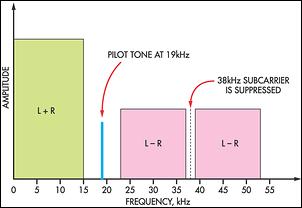
Fig.3: the frequency spectrum of the composite stereo FM signal. Note the spike of the pilot tone at 19kHz.
The outputs from the left and right LPFs are in turn applied to a multiplex (MPX) block. This is used to effectively produce sum (left plus right) and difference (left - right) signals which are then modulated onto a 38kHz carrier. The carrier is then suppressed (or removed) to provide a double-sideband suppressed carrier signal. It is then mixed in a summing (+) block with a 19kHz pilot tone to give a composite signal output (with full stereo encoding) at pin 5.
The phase and level of the 19kHz pilot tone are set using a capacitor at pin 19.
Fig.3 shows the spectrum of the composite stereo signal. The (L+R) signal occupies the frequency range from 0-15kHz. By contrast, the double sideband suppressed carrier signal (L-R) has a lower sideband which extends from 23-38kHz and an upper sideband from 38-53kHz. As noted, the 38kHz carrier is not present.
The 19kHz pilot tone is present, however, and this is used in the FM receiver to reconstruct the 38kHz subcarrier so that the stereo signal can be decoded.
The 38kHz multiplex signal and 19kHz pilot tone are derived by dividing down the 7.6MHz crystal oscillator located at pins 13 & 14. The frequency is first divided by four to obtain 1.9MHz and then divided by 50 to obtain 38kHz. This is then divided by two to derive the 19kHz pilot tone.
In addition, the 1.9MHz signal is divided by 19 to give a 100kHz signal. This signal is then applied to the phase detector which also monitors the program counter output. This program counter is actually a programmable divider which outputs a divided down value of the RF signal.
The division ratio of this counter is set by the voltage levels at inputs D0-D3 (pins 15-18). For example, when D0-D3 are all low, the programmable counter divides by 877. Thus, if the RF oscillator is running at 87.7MHz, the divided output from the counter will be 100kHz and this matches the frequency divided down from the 7.6MHz crystal oscillator (ie, 7.6MHz divided by 4 divided by 19).
Do you want to DIY make a 5w fm transmitter yourself ? Come with me, get our 5w fm transmitter PCB kit suite to DIY the 5w fm transmitter, click here

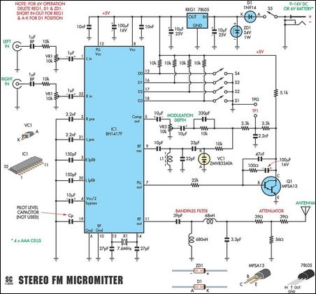
Fig.4: the complete circuit of the Stereo FM Micromitter. DIP switches S1-S4 set the RF oscillator frequency and this is controlled by the PLL output at pin 7 of IC1. This output drives Q1 which in turn applies a control voltage to VC1 to vary its capacitance. The composite audio output at pin 5 provides the frequency modulation.
In practice, the phase detector output at pin 7 produces an error signal to control the voltage applied to a varicap diode. This varicap diode (VC1) is shown on the main circuit diagram (Fig.4) and forms part of the RF oscillator at pin 9. Its frequency of oscillation is determined by the value of the inductance and the total parallel capacitance.
Do you want to DIY make a 5w fm transmitter yourself ? Come with me, get our 5w fm transmitter PCB kit suite to DIY the 5w fm transmitter, click here
Since the varicap diode forms part of this capacitance, we can alter the RF oscillator frequency by varying its value. In operation, the varicap diode's capacitance varies in proportion to the DC voltage applied to it by the output of the PLL phase detector.
In practice, the phase detector adjusts the varicap voltage so that the divided RF oscillator frequency is 100kHz at the program counter output. If the RF frequency drifts high, the frequency output from the programmable divider rises and the phase detector will "see" an error between this and the 100kHz provided by the crystal division.
As a result, the phase detector reduces the DC voltage applied to the varicap diode, thereby increasing its capacitance. And this in turn decreases the oscillator frequency to bring it back into "lock".
Conversely, if the RF frequency drifts low, the programmable divider output will be lower than 100kHz. This means that the phase detector now increases the applied DC voltage to the varicap to decrease its capacitance and raise the RF frequency. As a result, this PLL feedback arrangement ensures that the programmable divider output remains fixed at 100kHz and thus ensures stability of the RF oscillator.
By changing the programmable divider we can change the RF frequency. So, for example, if we set the divider to 1079, the RF oscillator must operate at 107.9MHz for the programmable divider output to remain at 100kHz.
Frequency modulation
Of course, in order to transmit audio information, we need to frequency modulate the RF oscillator. We do that by modulating the voltage applied to the varicap diode using the composite signal output at pin 5.
Note, however, that the average frequency of the RF oscillator (ie, the carrier frequency) remains fixed, as set by the programmable divider (or program counter). As a result, the transmitted FM signal varies either side of the carrier frequency according to the composite signal level - ie, it is frequency modulated.
Do you want to DIY make a 5w fm transmitter yourself ? Come with me, get our 5w fm transmitter PCB kit suite to DIY the 5w fm transmitter, click here
|
Bandpass Filter Option
We've designed the PC board so that it can accept a different bandpass filter at the pin 11 RF output of IC1. This filter is made by Soshin Electronics Co. and is labelled GFWB3. It is a small 3-terminal printed bandpass filter and operates in the 76-108MHz frequency band.
The advantage of using this filter is that it has much steeper rolloff above and below the FM band. This results in less sideband interference at other frequencies. The drawback is the filter is very difficult to obtain.
In practice, the filter replaces the 39pF capacitor, with the central earth terminal of the filter connecting to the PC board earth. That is why there is a hole between the 39pF capacitor leads. The 39pF and 3.3pF capacitors and the 68nH and 680nH inductors are then not required, while the 68nH inductor is replaced with a wire link.
|
Circuit details

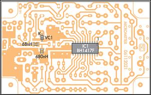
Fig.5(a): this diagram shows how the four surface-mount parts are installed on the copper side of the PC board. Make sure that IC1 & VC1 are correctly oriented.
Refer now to Fig.4 for the full circuit of the Stereo FM Micromitter. As expected, IC1 forms the main part of the circuitry with a handful of other components added to complete the FM stereo transmitter.
Do you want to DIY make a 5w fm transmitter yourself ? Come with me, get our 5w fm transmitter PCB kit suite to DIY the 5w fm transmitter, click here
The left and right audio input signals are fed in via 1μF bipolar capacitors and then applied to attenuator circuits consisting of 10kΩ fixed resistors and 10kΩ trimpots (VR1 & VR2). From there, the signals are coupled into pins 1 & 22 of IC1 via 1μF electrolytic capacitors.
Note that the 1μF bipolar capacitors are included to prevent DC current flow due to any DC offsets at the signal source outputs. Similarly, the 1μF capacitors on pins 1 & 22 are necessary to prevent DC current in the trimpots, since these two input pins are biased at half-supply. This half-supply rail is decoupled using a 10μF capacitor at pin 4 of IC1.
The 2.2nF pre-emphasis capacitors are at pins 2 & 21, while the 150pF capacitors at pins 3 & 20 set the low-pass filter rolloff point. The pilot level can be set with a capacitor at pin 19 - however, this is not usually necessary as the level is generally quite suitable without adding the capacitor.
In fact, adding a capacitor here only reduces the stereo separation because the pilot tone phase is altered compared to the 38kHz multiplex rate.
The 7.6MHz oscillator is formed by connecting a 7.6MHz crystal between pins 13 & 14. In practice, this crystal is connected in parallel with an internal inverter stage. The crystal sets the frequency of oscillation, while the 27pF capacitors provide the correct loading.

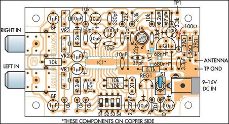
Fig.5(b): here's how to install the parts on the top of the PC board to build the plugpack-powered version. Note that IC1, VC1 and the 68nH & 680nH inductors are surface mount devices and are mounted on the copper side of the board as shown in Fig.5(a)
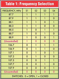
The programmable divider (or program counter) is set using switches at pins 15, 16, 17 & 18 (D0-D3). These inputs are normally held high via 10kΩ resistors and pulled low when the switches are closed. Table 1 shows how the switches are set to select one of 14 different transmission frequencies.
Do you want to DIY make a 5w fm transmitter yourself ? Come with me, get our 5w fm transmitter PCB kit suite to DIY the 5w fm transmitter, click here
The RF oscillator output is at pin 9. This is a Colpitts oscillator and is tuned using inductor L1, the 33pF & 22pF fixed capacitors and varicap diode VC1.
The 33pF fixed capacitor performs two functions. First, it blocks the DC voltage applied to VC1 to prevent current from flowing into L1. And second, because it is in series with VC1, it reduces the effect of changes in the varicap capacitance, as "seen" by pin 9.
This, in turn, reduces the overall frequency range of the RF oscillator due to changes in the varicap control voltage and allows better phase lock loop control.
Similarly, the 10pF capacitor prevents DC current flow into L1 from pin 9. Its low value also means that the tuned circuit is only loosely coupled and this allows a higher Q factor for the tuned circuit and easier starting of the oscillator.
Modulating the oscillator

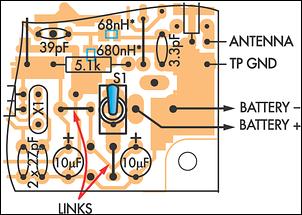
Fig.6: here's how to modify the board for the battery-powered version. It's just a matter of leaving out D1, ZD1 & REG1 and installing a couple of wire links.
The composite output signal appears at pin 5 and is fed via a 10μF capacitor to trimpot VR3. This trimpot sets the modulation depth. From there, the attenuated signal is fed via another 10μF capacitor and two 10kΩ resistors to varicap diode VC1.
As mentioned previously, the phase lock loop control (PLL) output at pin 7 is used to control the carrier frequency. This output drives high-gain Darlington transistor Q1 and this, in turn, applies a control voltage to VC1 via two 3.3kΩ series resistors and the 10kΩ isolating resistor.
The 2.2nF capacitor at the junction of the two 3.3kΩ resistors provides high-frequency filtering.
Additional filtering is provided by the 100μF capacitor and 100Ω resistor connected in series between Q1's base and collector. The 100Ω resistor allows the transistor to respond to transient changes, while the 100μF capacitor provides low-frequency filtering. Further high-frequency filtering is provided by the 47nF capacitor connected directly between Q1's base and collector.
The 5.1kΩ resistor connected to the 5V rail provides the collector load. This resistor pulls Q1's collector high when the transistor is off.
FM output
The modulated RF output appears at pin 11 and is fed to a passive LC bandpass filter. Its job is to remove any harmonics produced by the modulation and in the RF oscillator output. Basically, the filter passes frequencies in the 88-108MHz band but rolls off signal frequencies above and below this.
The filter has a nominal impedance of 75Ω and this matches both IC1's pin 11 output and the following attenuator circuit.
Two 39Ω series resistors and a 56W shunt resistor form the attenuator and this reduces the signal level into the antenna. This attenuator is necessary to ensure that the transmitter operates at the legal allowable limit of 10μW.
Do you want to DIY make a 5w fm transmitter yourself ? Come with me, get our 5w fm transmitter PCB kit suite to DIY the 5w fm transmitter, click here
Power supply

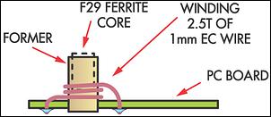
Fig.7: this diagram shows the winding details for coil L1. The former will have to be trimmed so that it sits no more than 13mm above the board surface. Use silicone sealant to holder the former in place, if necessary.
Power for the circuit is derived from either a 9-16V DC plugpack or a 6V battery.
In the case of a plugpack supply, the power is fed in via on/off switch S5 and diode D1 which provides reverse polarity protection. ZD1 protects the circuit against high-voltage transients, while regulator REG1 provides a steady +5V rail to power the circuit.
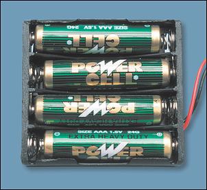
Alternatively, for battery operation, ZD1, D1 and REG1 are not used and the through connections for D1 and REG1 are shorted. The absolute maximum supply for IC1 is 7V, so 6V battery operation is suitable; eg 4 x AAA cells in a 4 x AAA holder.
Construction
A single PC board coded 06112021 and measuring just 78 x 50mm holds all the parts for the Micromitter. This is housed into a plastic case measuring 83 x 54 x 30mm.
First, check that the PC board fits neatly into the case. The corners may need to be shaped to fit over the corner pillars on the box. That done, check that the holes for the DC socket and RCA socket pins are the correct size. If L1's former doesn't have a base (see below), it is mounted by pushing it into a hole that is just sufficiently tight to hold it in place. Check that this hole has the correct diameter.
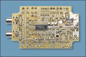
Fig.5(a) & Fig.5(b) show how the parts are mounted on the PC board. The first job is to install several surface-mount components on the copper side of the PC board. These parts include IC1, VC1 and two inductors.
You will need a fine-tipped soldering iron, tweezers, a strong light and a magnifying glass for this job. In particular, the soldering iron tip will have to be modified by filing it to a narrow screwdriver shape.

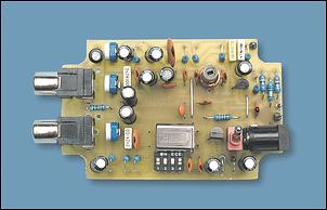
It's best to install the four surface-mount parts first (including the IC), before installing the remaining parts on the top of the PC board. Note how the body of the crystal lies across the two adjacent 10kΩ resistors (left photo).
IC1 and the varicap diode (VC1) are polarised devices, so be sure to orient them as shown on the overlay. Each part is installed by holding it in place with the tweezers and then soldering one lead (or pin) first. That done, check that the component is correctly positioned before carefully soldering the remaining lead(s).
In the case of the IC, it's best to first lightly tin the underside of each of its pins before placing it onto the PC board. It's then just a matter of heating each lead with the soldering iron tip to solder it in place.
Be sure to use a strong light and a magnifying glass for this work. This will not only make the job easier but will also allow you to check each connection as it is made. In particular, make sure that there are no shorts between adjacent tracks or IC pins.
Finally, use your multimeter to check that each pin is indeed connected to its respective track on the PC board.
The remaining parts are all mounted on the top side of the PC board in the usual manner. If you are building the plugpack-powered version, follow the overlay diagram shown in Fig.5. Alternatively, for the battery powered version, leave out ZD1 and the DC socket and replace D1 & REG1 with wire links as shown in Fig.6.
Do you want to DIY make a 5w fm transmitter yourself ? Come with me, get our 5w fm transmitter PCB kit suite to DIY the 5w fm transmitter, click here
Top assembly
Begin the top assembly by installing the resistors and wire links. Table 3 shows the resistor colour codes but we also recommend that you use a digital multimeter to check the values. Note that most of the resistors are mounted end-on to save space.
Once the resistors are in, install PC stakes at the antenna output and the TP GND and TP1 test points. This will make it much easier to connect to these points later on.
Next, install trimpots VR1-VR3 and the PC-mount RCA sockets. The DC socket, diode D1 and ZD1 can then be inserted for the plugpack-powered version.
The capacitors can go in next, taking care to install the electrolytic types with the correct polarity. The NP (non-polarised) or bipolar (BP) electrolytic types can be installed either way. Push them all the way down into their mounting holes, so that they sit no more than 13mm above the PC board (this is to allow the lid to fit correctly when the AAA batteries are mounted under the PC board inside the box).
The ceramic capacitors can also be installed at this stage. Table 2 shows their marking codes, to make it easy for you to identify the values.
Coil L1
Fig.7 shows the winding details for coil L1. It comprises 2.5 turns of 0.5 - 1mm enamelled copper wire (ECW) wound onto a tapped coil former fitted with an F29 ferrite slug. Alternatively, you may also use any commercially made 2.5 turns variable coil.
Two types of formers are available - one with a 2-pin base (which can be soldered directly to the PC board) and one that comes without a base. If the former has a base, it will first have to be shortened by about 2mm, so that its overall height (including the base) is 13mm. This can be done using a fine-toothed hacksaw.
That done, wind the coil, terminate the ends directly on the pins and solder the coil into position. Note that the turns are adjacent to each other (ie, the coil is close wound).

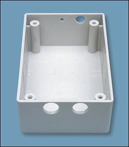
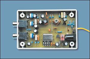
This photo shows how the case is drilled to take the RCA sockets, the power socket and the antenna lead.
Alternatively, if the former doesn't have a base, cut off the collar at one end, then drill a hole in the PC board at the L1 position so that the former is a tight fit. That done, push the former into its hole, then wind the coil so that the lowest winding sits on the top surface of board.
Be sure to strip away the insulation from the wire ends before soldering the leads to the PC board. A few dabs of silicone sealant can then be used to ensure that the coil former stays in place.
Finally, the ferrite slug can be inserted into the former and screwed in so that its top is about flush with the top of the former. Use a suitable plastic or brass alignment tool to screw in the slug - an ordinary screwdriver may crack the ferrite.
Crystal X1 can now be installed. This is mounted by first bending its leads by 90 degrees, so that it sits horizontally across the two adjacent 10kΩ resistors (see photo). The board assembly can now be completed by installing the DIP switch, transistor Q1, regulator (REG1) and the antenna lead.
The antenna is simply a half-wave dipole type. It consists of a 1.5m length of insulated hookup wire, with one end soldered to the antenna terminal. This should give good results as far as transmission range is concerned.
Do you want to DIY make a 5w fm transmitter yourself ? Come with me, get our 5w fm transmitter PCB kit suite to DIY the 5w fm transmitter, click here
Preparing
the case
Attention can now be turned to the plastic case. This requires holes at one end to accommodate the RCA sockets, plus holes at the other end for the antenna lead and the DC power socket (if used).
In addition, a hole must be drilled in the lid for the power switch.

The circuit can be powered from 4 x 1.5V AAA cells if you wish to make the unit portable. Note that the battery holder requires some modification in order to fit everything inside the case (see text).
It's also necessary to remove the internal side mouldings along the walls of the case to a depth of 15mm below the top edge of the box, in order to fit the PC board. We used a sharp chisel to remove these but a small grinder could be used instead. That done, you also need to remove the end ribs under the lid in order to clear the tops of the RCA and DC sockets. The front-panel label can then be attached to the lid.
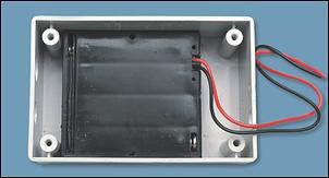
The battery-powered version has a AAA cell-holder mounted upside down in the box, with the base of the holder in contact with the copper side of the PC board. There is just sufficient room for this holder and the PC board to mount inside the case with the following provisos:
(1). All parts except for power switch S5 must not protrude above the surface of the PC board by more than 13mm. This means that the electrolytic capacitors must sit close to the PC board and that L1's former must be cut to the correct length.
(2). The AAA cell holder is about 1mm too thick and should be filed down at each end, so that the cells protrude slightly over the top of the holder.
(3). The tops of the RCA sockets may also require shaving slightly, so that there is no gap between the box and the lid after assembly.
|
ACA Compliance
This FM broadcast band stereo transmitter is required to comply with the Radiocommunications Low Interference Potential Devices (LIPD) Class Licence 2000, as issued by the Australian Communications Authority.
In particular, the frequency of transmission must be within the 88-108MHz band at a EIRP (Equivalent Isotropically Radiated Power) of 10mW and with FM modulation no greater than 180kHz bandwidth. The transmission must not be on the same frequency as a radio broadcasting station (or repeater or translator station) operating within the licence area.
Further information can be found on the www.aca.gov.au web site.
The class licence information for LIPDs can be downloaded from:
www.aca.gov.au/aca_home/legislation/radcomm/class_licences/lipd.htm
|
Test & adjustment
This part is a real snack. The first job is to tune L1 so that the RF oscillator operates over the correct range. To do that, follow this the step-by-step procedure:
(1). Set the transmission frequency using the DIP switches, as shown in Table 1. Note that you need to select a frequency that is not used as a commercial station in your area, otherwise interference will be a problem.
(2). Connect your multimeter's common lead to TP GND and its positive lead of to pin 8 of IC1. Select a DC volts range on the meter, apply power to the Micromitter and check that you get a reading that's close to 5V if you're using a DC plugpack.
Alternatively, the meter should show the battery voltage if you're using AAA cells.
(3). Move the positive multimeter lead to TP1 and adjust the slug in L1 for a reading of about 2V.

The battery holder sits in the bottom of the case, beneath the PC board.
The oscillator is now correctly tuned. No further adjustments to L1 should be required if you subsequently switch to another frequency within the selected band. However, if you change to a frequency that's in the other band, L1 will have to be readjusted for a reading of 2V at TP1.
Setting the trimpots
Do you want to DIY make a 5w fm transmitter yourself ? Come with me, get our 5w fm transmitter PCB kit suite to DIY the 5w fm transmitter, click here
Fig.8: the full-size front-panel artwork.
All that remains now is to adjust trimpots VR1-VR3 to set the signal level and modulation depth. The step-by-step procedure is as follows:
(1). Set VR1, VR2 & VR3 to their centre positions. VR1 and VR2 can be adjusted by passing a screwdriver through the centres of the RCA μ sockets, while VR3 can be adjusted by moving the μF capacitor in front of it to one side.
(2). Tune a stereo FM tuner or radio to the transmitter frequency. The FM tuner and transmitter should initially be placed about two metres apart.
(3). Connect a stereo signal source (eg, a CD player) to the RCA socket inputs and check that this is received by the tuner or radio.
Fig.9: full-size etching pattern for the PC board.
(4). Adjust VR3 anticlockwise until the stereo indicator goes out on the receiver, then adjust VR3 clockwise from this position by 1/8th of a turn.
(5). Adjust VR1 and VR2 for best sound from the tuner - you will have to temporarily disconnect the signal source to make each adjustment. There should be sufficient signal to "eliminate" any background noise but without any noticeable distortion.
Note particularly that VR1 and VR2 must each be set to the same position, to maintain the left and right channel balance.
That's it - your new Stereo FM Micromitter is ready for action.
|
Table 2: Capacitor Codes
| Value |
IEC Code |
EIA Code |
| 47nF |
47n |
473 |
| 10nF |
10n |
103 |
| 2.2nF |
2n2 |
222 |
| 330pF |
330p |
331 |
| 150pF |
150p |
151 |
| 39pF |
39p |
39 |
| 33pF |
33p |
33 |
| 27pF |
27p |
27 |
| 22pF |
22p |
22 |
| 10pF |
10p |
10 |
| 3.3pF |
3p3 |
3.3 |
|
|
Table 3: Resistor Colour Codes
| No. |
Value |
4-Band Code (1%) |
5-Band Code (1%) |
| 1 |
22kΩ |
red red orange brown |
red red black red brown |
| 8 |
10kΩ |
brown black orange brown |
brown black black red brown |
| 1 |
5.1kΩ |
green brown red brown |
green brown black brown brown |
| 2 |
3.3kΩ |
orange orange red brown |
orange orange black brown brown |
| 1 |
100Ω |
brown black brown brown |
brown black black black brown |
| 1 |
56Ω |
green blue black brown |
green blue black gold brown |
| 2 |
39Ω |
orange white black brown |
orange white black gold brown |
|
|
Parts List
1 PC board, code 06112021, 78 x 50mm.
1 plastic utility box, 83 x 54 x 31mm
1 front panel label, 79 x 49mm
1 7.6MHz or 7.68MHz crystal
1 SPDT subminiature switch (Jaycar ST-0300, Altronics S 1415 or equiv.) (S5)
2 PC-mount RCA sockets (switched) (Altronics P 0209, Jaycar PS 0279)
1 2.5mm PC-mount DC power socket
1 4-way DIP switch
1 2.5 turns variable coil (L1)
1 4mm F29 ferrite slug
1 680nH (0.68μH) surface mount inductor (1210A case) (Farnell 608-282 or similar)
1 68nH surface mount inductor (0603 case) (Farnell 323-7886 or similar)
1 100mm length of 1mm enamelled copper wire
1 50mm length of 0.8mm tinned copper wire
1 1.6m length of hookup wire
3 PC stakes
1 4 x AAA cell holder (required for battery operation)
4 AAA cells (required for battery operation)
3 10kΩ vertical trimpots (VR1-VR3)
Semiconductors
1 BH1417F Rohm surface-mount FM stereo transmitter (IC1)
1 78L05 low-power regulator (REG1)
1 MPSA13 Darlington transistor (Q1)
1 ZMV833ATA or MV2109 (VC1)
1 24V 1W zener diode (ZD1)
1 1N914, 1N4148 diode (D1)
Capacitors
2 100μF 16VW PC electrolytic
5 10μF 25VW PC electrolytic
2 1μF bipolar electrolytic
2 1μF 16VW electrolytic
1 47nF (.047μF) MKT polyester
2 10nF (.01μF) ceramic
3 2.2nF (.0022μF) MKT polyester
1 330pF ceramic
2 150pF ceramic
1 39pF ceramic
1 33pF ceramic
2 27pF ceramic
1 22pF ceramic
1 10pF ceramic
1 3.3pF ceramic
Resistors (0.25W, 1%)
1 22kΩ 1 100Ω
8 10kΩ 1 56Ω
1 5.1kΩ 2 39Ω
2 3.3kΩ
|
Do you want to DIY make a 5w fm transmitter yourself ? Come with me, get our 5w fm transmitter PCB kit suite to DIY the 5w fm transmitter, click here
|
Specifications
| Transmission frequencies |
87.7MHz to 88.9MHz in 0.2MHz steps
106.7MHz to 107.9MHz in 0.2MHz steps (14 total) |
| Total Harmonic Distortion (THD) |
typically 0.1% |
| Pre-emphasis |
typically 50ms |
| Low Pass Filter |
15kHz/20dB/decade |
| Channel separation |
typically 40dB |
| Channel balance |
within ?2dB (can be adjusted with trimpots) |
| Pilot modulation |
15% |
| RF Output power (EIRP) |
typically 10μW when using inbuilt attenuator |
| Supply voltage |
4-6V |
| Supply current |
28mA at 5V |
| Audio input level |
220mV RMS maximum at 400Hz and 1dB compression limiting |
|
|
The following downloads are available for this article:
|
Click here to buy Our DIY 5W PLL Digital LCD Stereo FM Transmitter PCB Kit Suite
Our other product:

