The development of radio frequency probes
Radio frequency (RF) probes play an important role in almost every stage of the life cycle of radio frequency products: from technology development, model parameter extraction, design verification and debugging all the way to small-scale production testing and final production testing. By using RF probes, it is possible to measure the true characteristics of RF components at the wafer level. This can shorten research and development time and greatly reduce the cost of developing new products.
In just thirty years, RF probe technology has made amazing progress, from low-frequency measurement to commercial solutions suitable for a variety of applications: such as impedance matching in 110GHz high-frequency and high-temperature environments, multi-port, differential and For mixed-signal measurement devices, high-power measurements up to 60W in continuous wave mode, and terahertz applications up to 750GHz, RF probes can be seen.
People’s earliest use of RF probe technology is very different from today’s tools. Early probes used a 50-Ω microstrip line that gradually converged from a short wire tip to pass through the probe substrate. A small hole is in contact with the pad of the device under test (DUT). At this time, the technical difficulty lies in how to achieve repeatable measurements when breaking through 4GHz. Although it is possible to eliminate the relatively large series inductance of a contact wire pole tip through the calibration process, when the wafer fixture is moved, the radiation impedance of the wire pole tip will change significantly. The pole tip design used for high frequency measurement is different from the pole tip used for DC and low frequency measurement, and the 50-Ω environment must be as close as possible to the DUT pressure point.
Mobile phone radio frequency module power amplifier (PA)
The power amplifier (PA) is used to amplify the radio frequency signal output by the transceiver. The power amplifier field is an independent field with thresholds. It is also a component that cannot be integrated in a mobile phone. It is also the most important component in a mobile phone. The performance of the mobile phone, the footprint, the call quality, the strength of the mobile phone, and the battery life are all determined by the power The amplifier decides.
The main manufacturers in the power amplifier field are RFMD, Skyworks, TriQuint, Renesas, NXP, Avago, ANADIGICS. Now, Qualcomm, which was originally a PA enterprise partner, has also directly joined the PA market. It will launch PA produced in CMOS process in the second half of 2013, supporting LTE-FDD, LTE-TDD, WCDMA, EV-DO, CDMA 1x , TD-SCDMA and GSM/EDGE seven modes, the spectrum will cover more than 40 frequency bands in global use, and announced its entry into the PA industry with the advantages of multi-frequency and multi-mode.
After the PA market has experienced the LDMS PA "challenge" era, gallium arsenide (GaAs) PA has become the "challenge" of the PA market in the 3G era. TriQuint, which led gallium arsenide to attack the PA market, is actively laying out the blueprint for gallium arsenide, launching a high-efficiency multi-frequency multi-mode power amplifier MMPA for the expansion of 3G/4G smart phones.
Qualcomm is attacking the PA market with CMOS PA. In the future, PA may become part of the mobile phone platform, and there will be a phenomenon of mobile phone chip platform companies acquiring and merging PA companies.
How to integrate these power amplifiers of different frequency bands and formats is an important topic that the industry has been studying. There are currently two solutions: one is a fusion architecture, which integrates radio frequency power amplifiers with different frequencies, and the other is an integration along the signal link, that is, PA and duplexers are integrated. The two schemes have their own advantages and disadvantages and are suitable for different mobile phones. Converged architecture, PA has a high degree of integration, which has obvious size advantages for more than 3 frequency bands, and has obvious cost advantages for 5-7 frequency bands. The disadvantage is that although the PA is integrated, the duplexer is still quite complicated, and there is switching loss when the PA is integrated, and the performance will be affected. For the latter architecture, the performance is better. The integration of the power amplifier and the duplexer can improve the current characteristics, which can save tens of milliamps of current, which is equivalent to extending the talk time by 15%. Therefore, the industry's suggestion is to use a converged architecture when there are more than 6 frequency bands (not counting 2G, but 3G and 4G), and when less than four frequency bands, use the PA and duplexer integrated solution PAD. At present, TriQuint can provide two kinds of architecture solutions, RFMD mainly prefers the architecture of fusion PA, and Skyworks prefers the multi-frequency PAD solution.
2.4G RF antenna debugging introduction and actual combat sharing
2019-8-26 16:16:18 Comment Report
keud
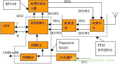
0Mobile phone radio frequency module RF transceiver
The transceiver is the core processing unit of the mobile phone radio frequency, which mainly includes the receiving unit and the transmitting unit. The former completes the amplification, filtering and down-conversion of the received signal and finally outputs the baseband signal. Usually adopt the way of zero intermediate frequency and digital low intermediate frequency to realize the conversion from radio frequency to baseband; the latter completes up-conversion, filtering, and amplification of baseband signals. Mainly adopt the way of twice frequency conversion to realize the conversion from baseband signal to radio frequency signal. When the radio frequency/intermediate frequency (RF/IF) IC receives the signal, the receiving unit receives the signal from the antenna (approximately 800Hz~3GHz) after amplifying, filtering and synthesizing, then the radio frequency signal is down-converted to baseband, followed by baseband signal processing ; When RF/IFIC transmits a signal, the baseband below 20KHz is up-converted, converted into a signal in the radio frequency band, and then transmitted.
In the past few years, manufacturers in the field of transceivers were divided into two major categories. One category relied on baseband platforms and used transceivers as part of the platform, such as Qualcomm, NXP, Freescale and MediaTek. This is because the transceiver has a very close relationship with the base frequency, and the two usually need to be designed in cooperation. The other category is professional RF manufacturers, such as Infineon, STMicroelectronics, and Skyworks, that do not rely on baseband platforms to expand the transceiver market.
With the development of transceivers towards integration and multi-mode, single-mode transceivers have been fully integrated into the base frequency. RF front-end devices of different frequency bands and formats have also been produced in different ways. Discrete RF transceivers are becoming rarer.
Mobile phone radio frequency front-end module (FEM)
The front-end module integrates a switch and a radio frequency filter to complete the switching of antenna receiving and transmitting, frequency band selection, and filtering of receiving and transmitting radio frequency signals. In the frequency band below 2GHz, many RF front-end modules are designed using complementary metal oxide semiconductor (CMOS), bipolar junction transistor (BJT), silicon germanium (SiGe), or Bipolar CMOS and other silicon integrated circuit manufacturing processes, which have gradually become mainstream. Since silicon integrated circuits have mature manufacturing processes, they are sufficient to design large and complex circuits, and they can be designed together with intermediate frequency and base frequency circuits, so they have great development potential. Other heterostructure transistors have also emerged in special-purpose circuits; however, in the frequency band above 5GHz, its performance in low noise characteristics, high power output, and power increase efficiency are far inferior to gallium arsenide field effect transistors. At this stage, arsenic The gallium field-effect transistor manufacturing process still has an advantage in the performance of electrical functions. RF front-end module circuit design has always focused on the design of power amplifiers, pursuing low-voltage operation, high-power output, and high-power efficiency to meet the use of low-voltage batteries, thereby reducing the size and meeting the requirements of power saving. Power increase efficiency and linearity are often inconsistent. However, under the extensive use of digital modulation technology, how to maintain good linearity has become an inevitable research focus.
For example, the high-integration smart phone front-end module that appeared in early 2013 covers the traditional GSM850, 900, 1800, and 1900 MHz frequency bands, as well as WCDMA frequency bands 1, 2, 4, and 5, and LTE frequency bands 2, 4, 5, and 5 Band 17. In addition to three surface acoustic wave filters and five duplexers, the module also contains a frequency band selection switch and decoder, and at the same time an ESD protection circuit that can protect up to 4 kV at the antenna output.
Mobile phone RF module development trend
As mobile phone manufacturers continue to develop mobile phones that support more frequency bands and streamlined radio frequency architectures, various frequency bands and air interface modules such as GSM, EDGE, WCDMA, and HSPA used in 3G mobile phones are integrated into a highly integrated and optimized RF Among the modules, it has become the first choice for 3G mobile phone design RF solutions.
The radio frequency (RF) front end in mobile phones will increasingly adopt integrated modules because it can simplify subsystems, reduce costs, and shrink size, add new functions to mobile phones, save space, and provide a single-chip front-end solution Create conditions. As front-end modules (FEMs) to radio frequency (RF) transceiver modules have been put into use one after another, the integration of mobile phone RF front-ends has continued to develop. In fact, as early as when the RF transceiver adopted a direct conversion or zero-intermediate frequency (ZIF) architecture (first eliminates the mid-frequency band and then eliminates the IF surface acoustic wave filter), front-end integration has already begun. With the evolution of transceiver architecture, external synthesis components (ie, voltage controlled oscillator and phase-locked loop) have been directly integrated in the transceiver chip. The high integration level achieves cost reduction and circuit board size reduction. The trend towards high integration shows no signs of stopping. However, since there are so many ways to integrate, it must be carefully considered in the design.
Qualcomm launched PA and improved its platform-based mobile phone solution is an example of integration. Previously, mobile phone platform solutions mainly included mobile phone baseband chips, application processors, radio frequency chips, power management and connection chips. PA was not included in the platform solutions, but had its own independent supplier. Qualcomm launched PA, more to make its solutions more ‘platform’
Afterwards, engineers made a breakthrough in probe technology. The basic requirements and working principles of radio frequency probes are determined:
1) The 50-Ω plane transmission line of the probe should directly contact the DUT pressure point without touching the wire. For the microstrip line and subsequent coplanar probe design, the contact of the probe is achieved with a small metal ball, which must be large enough to ensure reliable and repeatable contact.
2) In order to be able to contact the signal pressure point and ground pressure point of the DUT at the same time, the probe needs to be tilted. This process is called "probe planarization".
3) The contact repeatability of the probe is much better than that of the coaxial connector. Facilitate the development of probe tip and on-chip standards and special calibration methods.
4) The contact with high repeatability can perform accurate calibration of the probe and move the measurement reference plane to its extreme tip. The loss and reflection of the probe from the probe line and the transition to the coaxial connector are offset in a similar way by the error of the RF cable and the connector.
5) Due to its small geometric size, one can assume that the equivalent model of the plane standard part is purely lumped. In addition, people can easily predict model parameters from the geometric dimensions of standard parts.
As the probe design changes from microstrip lines to coplanar waveguides (CPW), probe manufacturing becomes very easy (Figure 1). Tektronix eventually transformed the probe from a "do it yourself" tool into a real product in the radio frequency semiconductor industry (Figure 2). This heralds the beginning of the era of RF measurement at the wafer level.
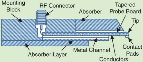
Figure 1. Wafer probe design based on ceramic coplanar lines
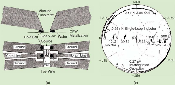
Figure 2. (a) Top view and side view of coplanar probe
(B) One-port measurement of various on-chip impedance standards after correction
In the early 1980s, Tektronix introduced the earliest RF wafer probe model TMP9600 and sapphire calibration substrate CAL96 (Figure 3). The main developers of the probe, Eric Strid and Reed Gleason, founded Cascade Microtech in 1983 and launched the WPH probe. These two companies provided very similar RF probes for several years, until Tektronix finally withdrew from the wafer probe business in the early 1990s. Under such an opportunity, CascadeMicrotech has become the most important supplier of RF probes in the industry by virtue of its good relationship with Hewlett Packard.
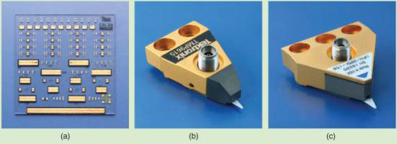
Figure 3. (a) The first commercial sapphire calibration substrate CAL96;
(B) RF wafer probe TMP9600 from Tektronix;
(C) WPH probe from Cascade Microtech.
The frequency of the WPH probe was expanded to 26 GHz in a short time, and reached 50 GHz in 1987 to meet the needs of the rapidly developed monolithic microwave integrated circuit (MMIC). V-band and W-band probes appeared in 1991 and 1993, respectively. In 1988, Cascade introduced the 26.5GHz series extremely tip replaceable probe (RTP) for large-scale production applications. Now, people can quickly replace the ceramic pole tip without moving the probe body from the test bench. WPH probes contributed to the development of microwave technology in the 1980s and 1990s, but there are several technical limitations. The most critical limitation is the fragile ceramic CPW wire. Even applying a minimum force above the recommended value (for example, to achieve better contact) will damage the probe. Many engineers refer to this moment as the "voice of death." The sound of cracking ceramic probes usually pushes the entire project to an end, because probes are very expensive for universities and small research labs. Although the RTP series was introduced, the ceramic probe was squeezed out of the market by other technologies.
When GGB Industries applied for a patent for a radio frequency probe based on a micro-coaxial cable, 1988 became another milestone. The use of micro coaxial cable as the intermediate transition medium has the following advantages:
1) Significant improvements in mechanical aspects extend the life of the probe.
2) The damaged probe can be tapped again in a relatively easy and inexpensive way.
3) The electrical characteristics have been improved.
4) Simplify the manufacturing process.
5) Reduce costs. In 1993, GGB introduced the W-band probe at the International Microwave Annual Conference (IMS) of the IEEE Theory and Technology Association. In 1999, their probes reached 220 GHz, in 2006 they were further expanded to 325 GHz, and in 2012 they reached 500 GHz. Coupled with close cooperation with suppliers such as Karl Suss (later SUSS MicroTech), GGB Industries has become one of the most influential companies in the world's RF market.
At the same time, Cascade demonstrated a new 40-GHz air-coplanar probe (ACP) at the 43rd Spring ARFTG Conference in 1994 (Figure 5). Within a few years, ACP probes quickly reached 110GHz (1-mm connector model) and 140GHz (based on waveguide model), replacing the WPH production line. So far, due to the soft and non-destructive contact of ACP, many engineers like to use ACP to detect gold pressure points.
Figure 4. Picoprobe probe from GGB Industries
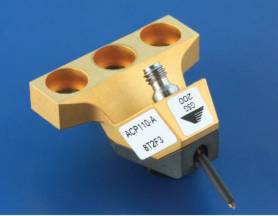
Figure 5, Cascade Microtech's ACP probe
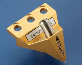
Figure 6. Z∣-probe model.
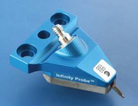
Figure 7. Infinity probe from Cascade Microtech
In 2000, Rosenberger introduced a new concept of RF probes for PCB applications, which significantly exceeded the traditional technology. The geometric size of the probes was reduced to the level required by the wafer level, and it was launched in 2001 New RF wafer probe ∣Z∣-probe. ∣Z∣-The probe can cover the 40GHz range and realize several innovative ideas.
1) This probe does not use micro coaxial cable. Realize the direct transition from coaxial connection to air-insulated coplanar contact wire.
2) This transition is made in the probe body, which allows an accurate optimization of the transition point, thereby minimizing possible discontinuities.
3) Coplanar contact is made using an ultraviolet lithography and electroplating process (UV-LIGA), which is similar to the process of making MEMS products. Its extremely high accuracy and repeatability can form a very accurate shape of CPW wire and a constant air gap.
In the mid-1990s, silicon was widely used in the radio frequency field. This brings some challenges to the production of radio frequency probes. Traditionally, the contact of the RF probe is made of beryllium-copper (BeCu). This material can become very troublesome when probing the aluminum contact pressure points of silicon devices and circuits. The rapid oxidation of the BeCu pole tip and the accumulation of dirt will lead to a great reduction in the repeatability of the contact pressure point of aluminum. To solve this problem, the supplier provides a radio frequency probe with a tungsten (W) pole tip. Test engineers who operate multi-purpose measuring devices are forced to change the probe every time the DUT type (silicon or III-V compound semiconductor) is changed, even if the frequency range of the test remains the same. ∣Z∣-probe is also committed to solving this inconvenience. Coplanar contact is made of nickel (Ni), which exhibits the best contact performance at the contact pressure points with aluminum and gold. Subsequently, other suppliers of radio frequency probes also began to provide multi-purpose probes made of Ni or Ni alloy to make pole tips.
With the growing demand for the radio frequency characteristics of MOS and BICMOS devices and the reduction of DUT contact size, Cascade Microtech introduced the microwave measurement conference based on the 59th Spring Automatic RF Techniques Group (ARFTG) in 2002. The new wafer probe for thin film technology. This method is based on Cascade's Pyramid Probe Card technology. The microstrip line on a soft polyimide film substrate transmits signals from the coaxial line to the DUT through the non-oxidized rare metal probe tip. The contact area of the Ni probe tip is approximately 12 μm x 12 μm, which can detect extremely small contact pressure points. This new Infinity probe demonstrates excellent contact consistency and very low probe-to-probe crosstalk.
Cascade company provides Infinity probes of different specifications that work below 110GHz. Waveguide-based probes for 220 and 325 GHz measurements were introduced in 2005 and 2007, respectively. Cascade started to provide Infinity probes for the 500GHz-band in late 2009.
During 2009-2011, two new members entered the mature probe market: DMPI with micromachining probes aimed at the emerging sub-THz market. Allstron from Taiwan provides inexpensive probes for applications below 110 GHz. Among them, the reduction of test costs is the most important requirement. The probe from Allstron is a traditional design based on micro-coaxial cable. The contact structure is an air-insulated CPW wire. It is similar to ACP, but the pole tip is made into a certain shape to detect aluminum pressure points with small passivation windows.
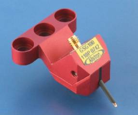
Figure 8. Radio frequency probe of Allstron
The modern design of RF wafer probes converts the test signal from a three-dimensional medium (coaxial cable or rectangular waveguide) to a two-dimensional (coplanar) probe contact. This kind of operation requires careful handling of the characteristic impedance Z0 of the transmission medium, and the correct conversion of electromagnetic energy between different propagation modes. Although the input of the wafer probe is a standardized coaxial or waveguide interface, its output (probe tip) can realize different design concepts. These interfaces, especially the probe tip, bring discontinuities into the measurement signal path. This discontinuity itself produces higher-order propagation modes. Therefore, the wafer probe and DUT excitation must only support a single quasi-TEM propagation mode and must exclude higher-order modes or exhibit higher impedance to higher-order modes.
The conversion of the EM field distribution map is maintained by several radio frequency transition measures in a single probe assembly. A traditional radio frequency probe is composed of the following parts:
1) The interface of the tester (coaxial or waveguide)
2) Transition from test interface to micro coaxial cable
3) Transition from micro coaxial cable to a planar waveguide, such as CPW or microstrip line
4) Several types of probes facing the coplanar interface (or pole tip) of the DUT on the wafer are either a combination of 3) and 4), or no micro-coaxial cable is used (Figure 9). A coaxial connector is a common test system interface for RF probes below 65 GHz. Both coaxial and waveguide connection schemes are possible interfaces in the frequency range of 50 to 110 GHz. In a single scan, the broadband test system covering from DC to 110GHz utilizes the smallest size (1mm) coaxial connector. Rectangular waveguides of different sizes are connected to measurement systems above 110 GHz.
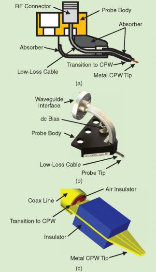
Figure 9. (a) Radio frequency detection based on a micro coaxial cable
(B) Waveguide interface
(C) Direct transition from coaxial to coplanar line
The natural life span of a probe technology is about 12 years. There are two main factors driving the development of probe technology:
1) Improve measurement accuracy in high-end applications
2) Reduce the test cost of mainstream applications.
In addition to the new probe suppliers for mainstream (Allstron) and high-end applications (DMPI), some small and medium-sized service providers in the RF and microwave industry are also providing products for low frequency and broadband fields.
The MP series coaxial probes provided by FindRF meet the measurement requirements of DC-20GHz. The characteristics are as follows:
1. DC-20GHz bandwidth
2. Ultra-low insertion and return loss
3. GSG, GS configuration (0.8/1.5/2.5mm pitch range)
Advantage:
1. Easy to detect and test the circuit board signal without any soldering
2. Compatible with pogo pins allowing exploration of non-planar structures
3. The service life of the probe is longer
4. Less testing time
Applied to:
1) RF and microwave module signal insertion, detection and measurement output;
2) Analysis of electrical performance of high-frequency circuit boards;
Our other product: