How to improve the efficiency of RF power amplifier?
The basic laws of thermodynamics reveal that no electronic equipment can achieve 100% efficiency-although switching power supplies are relatively close (up to 98%). Unfortunately, any device that generates RF power is currently unable to achieve or close to the ideal performance, because there are too many defects in the process of converting DC power into RF product power, including the loss caused by the entire signal path transmission, to the operating frequency Time loss, and the inherent characteristic loss of the device. As a result, an article in the MIT Technology Review unceremoniously commented on the RF power amplifier, "It is a very inefficient hardware."
Not surprisingly, every aspect of RF power product manufacturers, from semiconductors to amplifiers to transmitters, as well as universities and the Department of Defense, spend a lot of time and financial resources every year to improve the efficiency of RF power devices. There are good reasons for this: even a slight increase in efficiency can extend the working time of battery-powered products and reduce the annual power consumption of wireless base stations. Figure 1 shows the proportion of the RF part to the overall power consumption of the base station.
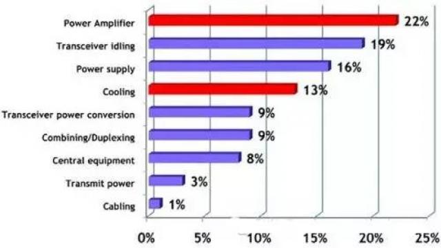
Figure 1: Adding the relevant parts of various radio frequency products in the power consumption of the base station, the final result will be quite large.
Fortunately, after years of continuous efforts to improve RF efficiency, these conditions are gradually changing. Some of these tasks are at the device level, while others use some innovative technologies, such as envelope tracking, digital predistortion / crest factor reduction schemes, and the use of amplifiers that are more advanced than common class AB levels.
A major shift in amplifier design is the Doherty architecture, which has become the standard for base station amplifiers within 5 years. Since Dr. Doherty of Bell Laboratories (which then became part of Westinghouse Electric) invented this architecture in 1936, it has been silent for most of the time and has only been used in a few applications.
Doherty's research has created a new amplifier structure that can provide extremely high power added efficiency when the input signal has a very high peak-to-average ratio (PAR). In fact, if properly designed, the efficiency of Doherty amplifiers can be increased by 11% to 14% compared to standard parallel class AB amplifiers.
Of course, for many years after 1936, only a few types of signals possess these characteristics, such as AM and FM, which use modulation schemes in communication systems. At present, almost every wireless system generates high PAR signals, from WCDMA to CDMA2000 to any system that uses orthogonal frequency division multiplexing (OFDM), such as WiMAX, LTE, and more recently, Wi-Fi.
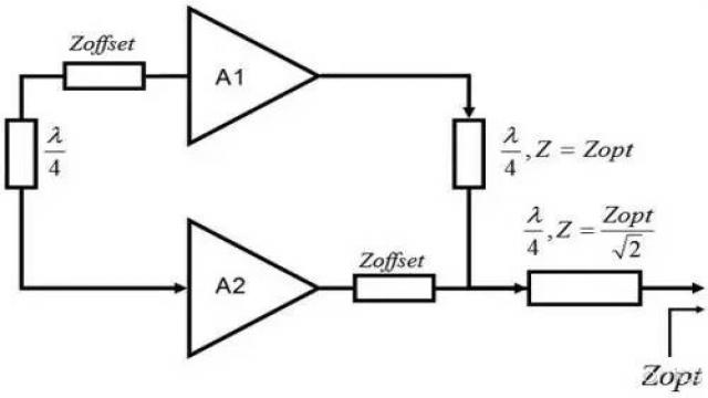
Figure 2: A typical Doherty amplifier
The classic Doherty amplifier (Figure 2), which can be classified as a load modulation architecture, is actually composed of two amplifiers: a carrier amplifier biased to operate in class AB mode, and a peak amplifier biased to class C mode. A power divider divides the input signal equally to each amplifier with a 90° phase difference. After amplification, the signal is re-synthesized through the power coupler. The two amplifiers operate at the same time when the input signal is at its peak, and each behaves as a load impedance to maximize output power.
However, as the input signal power drops, the Class C peak amplifier is turned off, and only the Class AB carrier amplifier still works. At lower power levels, the Class AB carrier amplifier behaves as a modulated load impedance to improve efficiency and gain. With the renewed vitality of the architecture, the Doherty amplifier design has made significant progress in rapid iterations and achieved great success.
Of course, no architecture is perfect. The linearity and output power of the Doherty amplifier are slightly worse than the dual class AB amplifier. This brings us another important circuit that has become an indispensable choice in today's communication environment: analog and digital linearization technology. The most widely used of this technology is digital predistortion (DPD), sometimes combined with crest factor reduction (CFR). Both DPD and CFR can greatly reduce Doherty's distortion, and careful device and amplifier design can minimize linearity loss. However, they are not strictly defined for use in Doherty amplifiers, and their effects are quite obvious when used in other amplifier structures.
1. Improve linearity
Modern digital modulation technology requires that the linearity of the amplifier is sufficiently high, otherwise intermodulation distortion will occur and the signal quality will be reduced. Unfortunately, when the amplifiers perform at their best, they are all close to their saturation levels. Later, they become non-linear, the RF power output drops as the input power increases, and significant distortions begin to appear. This distortion can cause crosstalk between adjacent channels or services. As a result, designers usually back off the RF output power to a "safe zone" to ensure linearity. When they do this, multiple RF transistors are necessary to achieve a given RF output power, which will increase current consumption and result in shorter battery life or higher operating costs in base stations.
DPD effectively introduces "anti-distortion" at the input of the amplifier, eliminating the amplifier's nonlinearity. As a result, the amplifier does not need to fall back to the optimal operating point, and thus no more RF power devices are required. As amplifiers become more efficient, the benefits are reduced cooling costs and all important power consumption. When CFR is working, the distortion is continuously checked by reducing the peak-to-average ratio of the input signal. This method reduces the peak value of the signal so that the signal does not cause clipping or distortion when passing through the amplifier. When DPD and CFR are used together, greater gain can be achieved.
2. Out-of-phase power amplifier method
Another technology is a patented technology invented and held by Henri Chireix nearly 80 years ago. It is usually called "outphasing" (outphasing power amplifier, a member of the load modulation technology family). It is currently used by Fujitsu, NXP, etc. To improve amplifier efficiency. It combines two non-linear RF power amplifiers, which are driven by signals of different phases. Because the phase is controlled, when the output signal is coupled, the use of Class B RF power amplifiers can achieve efficiency gains. Careful design techniques, especially selecting the appropriate reactance, can optimize the system to a specific output amplitude, which will bring twice the efficiency increase (at least in theory).
Fujitsu announced last year that it has adopted the outphasing method in a certain power amplifier, integrating a compact, low-loss power coupling circuit, and with a DSP-based phase error correction compensation circuit, which is 65% of the transmission time common to existing amplifiers. , The transmission time of the amplifier can exceed 95%. To test the design, the peak output of this power amplifier can reach 100 watts; the average electrical efficiency is increased from 50% to 70%.
The input signal is divided into two signals with constant amplitude and phase changes. The amplitude is set according to the RF power device, and the power coupling circuit reconstructs the source signal waveform. Previously, when the source signal was reconstructed, the loss of coupling accuracy needed to determine the phase difference, which prevented the commercialization of this technology. The coupler used by Fujitsu has a shorter signal path, which reduces loss and increases bandwidth.
3. NXP's promising development
A variant of the Outphasing mechanism without load modulation effect is called Linear Amplifier of Nonlinear Concept (LINC), which uses a separate coupler and amplifier stage to drive to saturation, and can effectively improve linearity and peak efficiency. However, the efficiency of LINC amplifiers is relatively low, because each amplifier operates at a constant power, even at low RF output levels. Chireix corrected this by combining outphasing with a non-separated coupler and load modulation to increase the average efficiency. NXP Semiconductors has made a further improvement, using outphasing to control two switch-mode RF amplifiers to adapt them to high crest factor signals. The company is combining Chireixoutphasing technology with GaN HEMT switching Class E amplifiers (Figure 3).
Figure 3: Simplified Chireix out-of-phase power amplifier block diagram
The new driver technology developed and patented by NXP enables the amplifier to achieve high efficiency over a bandwidth of approximately 25% by controlling the phase relationship. This has led to a new architecture that combines Class E amplifiers and load modulation to maintain the high efficiency of the amplifiers when they exit saturation, which allows them to adapt to various complex waveforms. NXP provided a reference design for the E-class RF power amplifier based on GaN devices, and attached Chireix related technical information.
4. Envelope tracking
Another key technology that amplifier designers pay attention to is envelope tracking. In this technology, the voltage applied to the power amplifier is continuously adjusted to ensure that it works in the peak region to maximize power. Compared with the fixed voltage provided by the DC-DC converter in a typical power amplifier design, the envelope tracking power supply modulates the power supply connected to the amplifier with a high-bandwidth, low-noise waveform, which is synchronized to the instantaneous envelope signal.
The use of envelope tracking technology in CMOS RF power devices has considerable appeal. Nujira has been developing this technology for many years. They have shown that this technology can overcome the shortcomings caused by non-linearities in CMOS RF amplifier applications. CMOS power amplifiers have been criticized as a bad choice for current high PAR modulation technology because of their inherent poor linearity, which requires them to fall back to reduce distortion. When CMOS amplifiers are operated at higher RF power levels, clipping and distortion will occur.
However, Nujira combines its patented ISOGAIN linearization technology in its proprietary envelope tracking technology to eliminate linearity problems without using DPD. The equipment using this technology has reached the goal of high efficiency and has achieved the same performance as GaAs in other aspects. A huge benefit of all research on CMOS amplifiers is that CMOS devices are ubiquitous in the entire electronics industry, supported by many foundries, so they are relatively cheap. Because it is based on silicon, it is also possible to directly integrate control and bias circuits on the power amplifier chip.
5. Other completely different methods
Another amplifier technology was advocated by Eta Devices, a company spun off from the Massachusetts Institute of Technology, and was co-founded by two electrical engineering professors Joel Dawson and David Perreault and a former amplifier researcher from Ericsson and Huawei. Its Asymmetric Multi-Level Outphasing (AMO) technology was developed by MIT, which was jointly invested by ADI co-founder Ray Stata and his venture capital firm Stata Venture Partners.
The company's primary target is emerging markets, including as many as 640,000 diesel generator power base stations that cost US$15 billion per year in terms of fuel, followed by the smartphone market. In February this year, Eta Devices demonstrated its Eta5 equipment at the Advanced LTE section of the Mobile Communications World Congress in Barcelona, Spain. The transmission channel of the equipment exceeds 80-MHz.
Eta Devices boldly declared that its ETAdvanced (Advanced Envelope Tracking) technology is expected to reduce base station energy costs by 50%. It also claims that it can double the battery life of smartphones. The premise is that the RF power transistor of the amplifier consumes power consumption simultaneously in the standby mode and the transmit mode, and the only way to improve efficiency is to reduce the standby power to the lowest possible level.
Switching between low power consumption standby mode and high power output will cause distortion. Existing systems need to maintain a high standby power level in order to continuously detect this condition, at the cost of high power consumption. Eta Devices' approach is to select the voltage that consumes the lowest power consumption across the transistor by sampling up to 20 million times per second.
Another problem is that the company explained that the LTE Advanced and 100 MHz bandwidth requirements will create huge demand for RF power amplifiers. Envelope tracking alone cannot adapt to this situation, because it cannot support channels wider than 40Mhz. According to the company, ETAdvanced supports channels up to 160 MHz, so it can meet both LTE-Advanced and 802.11ac Wi-Fi. Base stations using its technology can be very small, and the company claims that it has developed the first LTE transmitter with an average efficiency greater than 70%.
6. Summary
If you fully describe the current work done to improve RF power efficiency, you can write a large book. These contents are not limited to the scope discussed in this article, but also include the use of different types of amplifiers and supporting technologies. The combination of these technologies can produce meaningful results. No matter how much progress is made, it is certain that as long as the demand for higher data rates still exists, the search for higher efficiency will continue.
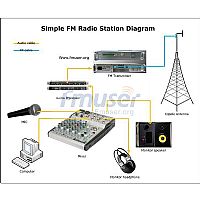
Our other product: