Realization of wireless system using RF power amplifier driver
At present, 8Vpp and pulse width modulation RF high-voltage/high-power drivers can be realized on the basis of 1.2V 65nm CMOS technology. Within the operating frequency range of 0.9 to 3.6GHz, the chip can provide a maximum output swing of 8.04Vpp to a 50Ω load at a 9V operating voltage. This allows CMOS drivers to directly connect and drive power transistors such as LDMOS and GaN. The maximum on-resistance of this driver is 4.6Ω. The duty cycle control range measured at 2.4GHz is 30.7% to 71.5%. By using a new thin oxide layer drain extension MOS device, the driver can achieve reliable high-voltage operation, and this new device does not require additional costs when implemented by CMOS technology.
Modern wireless handheld communication radios (including radio frequency (RF) power amplifiers (PA)) are all implemented in deep submicron CMOS. However, in wireless infrastructure systems, due to the need for larger output power levels, it is necessary to achieve RF PA through silicon LDMOS or hybrid technologies (such as GaA and more advanced GaN). For the next generation of reconfigurable infrastructure systems In other words, the switch mode PA (SMPA) seems to provide the required flexibility and high performance for multi-band multi-mode transmitters. However, in order to connect the high-power transistors used in the SMPA of the base station to all the digital CMOS modules of the transmitter, a broadband RF CMOS driver capable of generating a high voltage (HV) swing is required. This not only can achieve better high-power transistor performance, but also can directly use digital signal processing to control the required SMPA input pulse waveform, thereby improving the overall performance of the system.
Design challenge
The input capacitance of LDMOS or GaN SMPA is usually several picofarads and must be driven by a pulse signal with an amplitude higher than 5Vpp. Therefore, the SMPA CMOS driver must provide both high voltage and watt-level RF power. Unfortunately, deep sub-micron CMOS poses many challenges to the realization of high-voltage and high-power amplifiers and drivers, especially the extremely low maximum operating voltage (ie, low breakdown voltage caused by reliability issues) and passive passives with large losses. Devices (for example for impedance transformation).
Existing solutions
There are not many methods for implementing high-voltage circuits. Technical solutions (such as multi-gate oxide) that can realize high-voltage tolerance transistors can be used, but the cost is that the production process is expensive, and additional masks and processing steps must be added to the baseline CMOS process, so this solution is not ideal. In addition, in order to reliably increase the high voltage tolerance, a circuit scheme using only standard base line transistors (using thin/thick oxide devices) can be used. In the second method, device stacking or series cathodes are the most common examples. However, the complexity and performance of RF have great limitations, especially when the number of series-connected cathode (or stacked) devices increases to 2 or more. Another way to implement high-voltage circuits is to use drain-extended field effect transistors (EDMOS) in baseline CMOS technology as described in this article.
New solution
The drain extension device is based on intelligent wiring technology, which benefits from the realization of very fine dimensions in the ACTIVE (silicon), STI (oxide) and GATE (polysilicon) regions, and the use of baselines without additional costs Deep sub-micron CMOS technology realizes two high-voltage tolerance transistors, PMOS and NMOS. Although the RF performance of these EDMOS devices is actually lower compared to standard transistors using this process, they can still be used in the entire high-voltage circuit due to the elimination of important loss mechanisms associated with other HV equivalent circuits (such as series cathodes) To achieve higher overall performance.
Therefore, the high-voltage CMOS driver topology described in this article uses EDMOS devices to avoid device stacking. The RF CMOS driver adopts thin oxide layer EDMOS devices and is manufactured through a 65nm low standby power baseline CMOS process, and no additional mask steps or processes are required. For PMOS and NMOS, the fT measured on these devices exceeds 30GHz and 50GHz, respectively, and their breakdown voltage is limited to 12V. High-speed CMOS drivers have unprecedentedly achieved an output swing of 8Vpp up to 3.6GHz. Such a wide band gap-based SMPA provides driving.
Figure 1 is a schematic diagram of the structure of the driver described herein. The output stage includes an EDMOS-based inverter. EDMOS devices can be directly driven by low-voltage high-speed standard transistors, which simplifies the integration of the output stage and other digital and analog CMOS circuits on a single chip. Each EDMOS transistor is driven by a tapered buffer (buffer A and B in Figure 1) implemented by 3 CMOS inverter stages. The two buffers have different DC levels to ensure that each CMOS inverter can operate stably at a voltage of 1.2V (limited by technology, that is, VDD1-VSS1=VDD0-VSS0=1.2V). In order to use different power supply voltages and allow the same AC operation, the two buffers have exactly the same structure and are built into a separate Deep N-Well (DNW) layer. The output swing of the driver is determined by VDD1-VSS0, and any value that does not exceed the maximum breakdown voltage of the EDMOS device can be selected at will, while the operation of the internal driver remains unchanged. The DC level shift circuit can separate the input signal of each buffer.
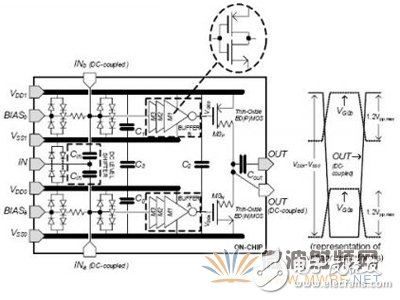
Figure 1. Schematic diagram of RF CMOS drive circuit and corresponding voltage waveforms.
Another function of the CMOS driver is to control the pulse width of the output square wave, which is realized by pulse width modulation (PWM) through variable gate bias technology. PWM control helps to achieve fine-tuning and tuning functions, thereby enhancing the performance of advanced SMPA devices. The bias level of the first inverter (M3) of the buffers A and B can move up/down the RF sinusoidal input signal with reference to the switching threshold of the inverter itself. The change of the bias voltage will change the output pulse width of the inverter M3. Then, the PWM signal will be transmitted through the other two inverters M2 and M1 and combined in the output stage (EDMOS) of the RF driver.
Our other product: