Chip design is one of the development priorities of each country, and expanding China's chip design industry will help reduce my country's dependence on foreign chips. In previous articles, the editor once introduced the forward and reverse flow of chip design and the prospects of chip design. In this article, the editor will introduce to you the actual chip design chapter-the optimization and realization of the clock tree power consumption in the RFID chip design.
1 Overview
UHF RFID is a UHF radio frequency identification tag chip. The chip adopts a passive power supply mode: after receiving the carrier energy, the RF front-end unit generates a Vdd power signal to supply the entire chip to work. Due to the limitations of the power supply system, the chip cannot generate a large current drive, so low-power design has become a major breakthrough in the chip development process. In order to make the digital circuit part produce as little power consumption as possible, in the digital logic circuit design process, in addition to simplifying the system structure (simple functions, only contains the encoding module, decoding module, random number generation module, clock, reset module, memory control unit As well as the overall control module), asynchronous circuit design is adopted in the design of some circuits. In this process, we saw that because the clock tree consumes a large part of the power consumption of the digital logic (about 30% or more), reducing the power consumption of the clock tree has also become a reduction in the power consumption of the digital logic and the power of the entire tag chip. An important step for consumption.
2 Chip power composition and methods to reduce power consumption
2.1 The composition of power consumption
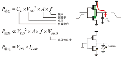
Figure 1 Composition of chip power consumption
Dynamic power consumption mainly includes short-circuit power consumption and flipping power consumption, which are the main components of the power consumption of this design. The short-circuit power consumption is the internal power consumption, which is caused by the instantaneous short circuit caused by the P tube and the N tube being turned on at a certain moment in the device. Turnover power consumption is caused by the charging and discharging of the load capacitance at the output of the CMOS device. Leakage power consumption mainly includes power consumption caused by subthreshold leakage and gate leakage.
Today, the two most important sources of power consumption are: capacitance conversion and subthreshold leakage.
2.2 Main methods to reduce power consumption
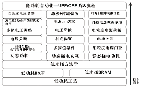
Figure 2 Main methods to reduce chip power consumption
2.2.1 Reduce the power supply voltage Vdd
Voltage Island: Different modules use different power supply voltages.
MulTI-level Voltage Scaling: There are multiple voltage sources in the same module. Switch between these voltage sources according to different applications.
Dynamic Voltage Frequency Scaling: The upgraded version of "multi-level voltage adjustment", which dynamically adjusts the voltage according to the working frequency of each module.
AdapTIve Voltage Scaling: An upgraded version of DVFS that uses a feedback circuit that can monitor circuit behavior to adjust the voltage adaptively.
Sub-threshold circuit (the design is more difficult, and it still stays in the scope of academic research)
2.2.2 Reduce frequency f and turnover rate A
Code optimization (extracting common factors, resource reuse, operand isolaTIon, serial work to reduce peak power consumption, etc.)
Gated clock
Multi-clock strategy
2.2.3 Reduce load capacitance (CL) and transistor size (Wmos)
Reduce sequential units
Chip area and scale reduction
Process upgrading
2.2.4 Reduce leakage current Ileak
Control threshold voltage (Threshold Voltage) (threshold voltage ↑ leakage current ↓ if using MTCMOS, VTCMOS, DTCMOS)
Control the gate voltage (Gate Voltage) (by controlling the gate-source voltage to control the leakage current)
Transistor Stack (connect redundant transistors in series, increase resistance to reduce leakage current)
Gated power supply (Power gaTIng or PSO) (when the module is not working, turn off the power to effectively reduce the leakage current)
3 Optimization of clock tree power consumption in RFID chip
When the chip is working, a large part of the power consumption is due to the turnover of the clock network. If the clock network is large, the power loss caused by this part will be very large. Among many low-power technologies, the gated clock has the strongest restraint effect on the flip power consumption and internal power consumption. In this design, the combination of multi-level gated clock technology and a special clock tree optimization strategy save a large part of power consumption. This project used a variety of optimization strategies for power consumption in the logic design, and tried some methods in the back-end synthesis and physical design. Through several power optimization and iterations in the front and back ends, the logic code design and the minimum power consumption were found Integrated approach.
4.1 Manually add clock gating in RTL stage
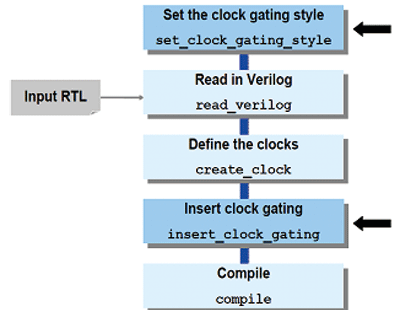
Figure 3 Schematic diagram of gated clock
module data_reg (En, Data, clk, out)
input En, clk;
input [7:0] Data;
output [7:0] out;
always @(posedge clk)
if (En) out = Data;
endmodule
The purpose of this stage is mainly twofold: The first is to add a gated clock unit to control the turnover rate and reduce the dynamic power consumption more reasonably according to the clock turnover probability of each module. The second is to produce a clock network with a balanced structure as much as possible. It can be guaranteed that some clock buffers can be added in the synthesis stage of the back-end clock tree to reduce power consumption. The ICG (Integrated Gating) unit in the foundry cell library can be directly used in the actual code design.
4.2 The tools in the synthesis phase are inserted into the integrated gate
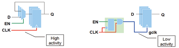
Figure 4 Gated clock insertion during logic synthesis
#Set clock gating options, max_fanout default is unlimited
set_clock_gating_style -sequential_cell latch \
-positive_edge_logic {integrated} \
-control_point before \
-control_signal scan_enable
#Create a more balanced clock tree by inserting “always enabled” ICGs
set power_cg_all_registers true
set power_remove_redundant_clock_gates true
read_db design.gtech.db
current_design top
link
source design.cstr.tcl
#Insert clock gating
insert_clock_gating
compile
#Generate a report on clock gating inserted
report_clock_gating
The purpose of this stage is to use the integrated tool (DC) to automatically insert the gated unit in order to further reduce power consumption.
It should be noted that the parameter settings for inserting ICG, such as maximum fanout (the larger the fanout, the more power saving, the more balanced the fanout, the smaller the skew, depending on the design, as shown in the figure), and the minimum_bitwidth parameter setting In addition, it is necessary to insert a normally open ICG for more complex gate control structures to make the clock network structure more balanced.
4.3 Optimizing power consumption at the synthesis stage of the clock tree
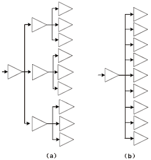
Figure 5 Comparison of two clock tree structures (a): multi-level depth type; (b): few-level flat type
First introduce the influence of the comprehensive parameters of the clock tree on the structure of the clock tree:
Skew: Clock skew, the overall goal of the clock tree.
Insertion delay (Latency): The total delay of the clock path, used to limit the increase in the number of levels of the clock tree.
Max taranstion: The maximum conversion time limits the number of buffers that can be driven by the first-level buffer.
Max Capacitance Max Fanout: The maximum load capacitance and maximum fanout limit the number of buffers that can be driven by the first-level buffer.
The final goal of clock tree synthesis in general design is to reduce clock skew. Increasing the number of levels and reducing each level of fanout will invest more buffers and more accurately balance the latency of each clock path to obtain a smaller skew. But for low-power design, especially when the clock frequency is low, the timing requirements are not very high, so it is hoped that the scale of the clock tree can be reduced to reduce the dynamic switching power consumption caused by the clock tree. As shown in the figure, by reducing the number of levels of the clock tree and increasing fanout, the size of the clock tree can be effectively reduced. However, due to the reduction in the number of buffers, a clock tree with a smaller number of levels than a multi-level clock tree Just roughly balance the latency of each clock path, and get a larger skew. It can be seen that with the goal of reducing the scale of the clock tree, low-power clock tree synthesis is at the expense of increasing a certain skew.
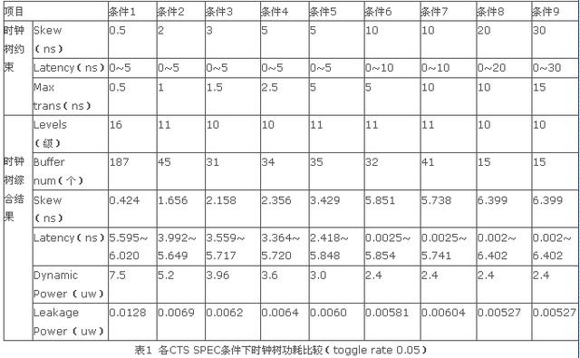
Specifically for this RFID chip, we use TSMC 0.18um CMOS LOGIC/MS/RF process, and the clock frequency is only 1.92M, which is very low. At this time, when the clock is used for clock tree synthesis, the low clock is used to reduce the scale of the clock tree. The power consumption clock tree synthesis mainly sets the constraints of skew, latency and transiton. Since restricting fanout will increase the number of clock tree levels and increase the power consumption, this value is not set. The default value in the library. In practice, we have used 9 different clock tree constraints, and the constraints and comprehensive results are shown in Table 1.
5 Conclusion
As shown in Table 1, the general trend is that the larger the target skew is, the smaller the final clock tree size, the smaller the number of clock tree buffers, and the smaller the corresponding dynamic and static power consumption. This will save the clock tree. The purpose of consumption. It can be seen that when the target skew is greater than 10ns, the power consumption basically does not change, but the large skew value will bring about the deterioration of the hold timing and increase the number of buffers inserted when repairing the timing, so a compromise should be made. From the chart Strategy 5 and Strategy 6 are the preferred solutions. In addition, when the optimal skew setting is selected, you can also see that the larger the Max transition value is, the lower the final power consumption is. This can be understood as the longer the clock signal transition time, the smaller the energy required. In addition, the setting of the latency constraint can be enlarged as much as possible, and its value has little effect on the final power consumption result.
Our other product: