Radio frequency circuit of low power consumption passive ultrahigh frequency radio frequency identification transponder chip
This paper proposes a high-performance low-power passive ultra-high frequency (UHF) radio frequency identification (RFID) transponder chip radio frequency circuit that meets the ISO/IEC18000-6B standard. The radio frequency circuit has no external components except the antenna, and receives energy from the radio frequency electromagnetic field through a Schottky diode rectifier.
Network engineer electronic enthusiasts • Source: Site finishing • Author: Anonymous • 2010 Nian 01 Yue 26 Ri 11:14 • 648 Read 0 times
Radio frequency circuit of low power consumption passive ultrahigh frequency radio frequency identification transponder chip
This paper proposes a high-performance low-power passive ultra-high frequency (UHF) radio frequency identification (RFID) transponder chip radio frequency circuit that meets the ISO/IEC18000-6B standard. The radio frequency circuit has no external components except the antenna, and receives energy from the radio frequency electromagnetic field through a Schottky diode rectifier.
0 Preface
Radio frequency identification (RFID) is an automatic identification technology that emerged in the 1990s. RFID technology has a variety of advantages that bar code technology does not have, and it has a wide range of applications. It can be applied to second-generation citizen ID cards, city card, financial transactions, supply chain management, electronic publication fees (ETC), access control, airport Baggage management, public transportation, container identification, livestock management, etc. Therefore, it is very important to master the technology of manufacturing RFID chips. At present, the ever-increasing application demand puts forward higher requirements on RFID chips, which require larger capacity, lower cost, smaller volume, and higher data rate. According to this situation, this article proposes a long-distance, low-power passive UHF UHF RFID transponder chip radio frequency circuit.
Common working frequencies of RFID include low frequency 125kHz, 134.2kHz, high frequency 13.56MHz, UHF 860~930MHz, microwave 2.45GHz, 5.8GHz, etc. Because the low frequency 125kHz, 134.2kHz, high frequency 13.56MHz system uses coils as antennas and uses inductors The working distance is relatively short, generally no more than 1.2m, and the bandwidth is limited to several kilohertz in Europe and other regions. However, UHF (860~93Uh1Hz) and microwave (2.45GHz, 5.8GHz) can provide longer working distance, higher data rate, and smaller antenna size, so it has become a hot research field of RFID.
The RF circuit chip proposed in this paper is taped out using the Chartered 0.35μm 2P4M CM0S process that supports Schottky diodes and electrically erasable programmable read-only memory (EEPROM). Schottky diodes have lower series resistance and forward voltage, and can provide higher conversion efficiency when converting the received RF input signal energy into a DC power supply, thereby reducing power consumption. When the effective isotropic radiated power (EIRP) is 4W (36dBm) and the antenna gain is 0dB, the radio frequency circuit chip works at 915MHz, the reading distance is greater than 3m, and the working current is less than 8μA.
1 RF circuit structure
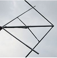
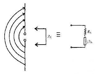
Figure 1 is the UHF RF1D transponder chip system diagram, which mainly includes radio frequency circuits, logic control circuits and EEPROM. Among them, the radio frequency circuit part can be divided into the following main circuit modules: local oscillator and clock generation circuit, power-on reset circuit, voltage reference source, matching network and backscatter circuit, rectifier, voltage regulator and amplitude modulation ( AM) Demodulator, etc. There are no external components except the antenna, and the antenna part adopts a dipole structure, and is matched with the input impedance of the rectifier through a matching network, as the only energy source for the entire chip. The equivalent model is shown in Figure 2. The real part of the impedance of a dipole antenna consists of two parts, Rra and Rloss, where Rra is the radiation impedance of the dipole antenna, which is inherent to the dipole antenna, generally 73Ω, which represents the ability of the antenna to radiate electromagnetic waves to the outside; Rloss The ohmic resistance of the metal used to make the antenna generally only generates heat. The imaginary part X of the antenna impedance is generally positive. This is because the antenna is generally inductive to the outside. The magnitude of the equivalent inductance generally depends on the topological structure of the antenna and the substrate material. The rectifier converts the coupled RF input signal power into the DC voltage required by the chip. The voltage regulator stabilizes the DC voltage at a certain level and limits the amplitude of the DC voltage to protect the chip from breakdown due to excessive voltage. The AM demodulator is used to extract the corresponding data signal from the received carrier signal. The backscatter circuit uses a variable capacitor to change the impedance of the radio frequency circuit, thereby sending the transponder data to the RFID interrogator or card reader. The power-on reset circuit is used to generate a reset signal for the entire chip. Unlike the 13.56MHz high frequency (HF) transponder, the 915MHz UHF transponder cannot obtain a local clock from the carrier frequency, but can only provide a clock for the digital logic circuit part through a built-in low-power local oscillator. All these circuit modules will be described in detail below one by one.
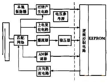
Figure 1 UHF RF1D transponder chip system diagram
2 Equivalent electrical model of transponder antenna
2 Circuit design and analysis
2.1 Rectifier and regulator circuit
In this paper, a Dickson charge pump composed of Schottky diodes is used as the rectifier circuit. The schematic diagram of the circuit is shown in Figure 3. This is because Schottky diodes have lower series resistance and junction capacitance, and can provide higher conversion efficiency when converting the received RF input signal energy into a DC power supply, thereby reducing power consumption. All Schottky diodes are connected together by poly-poly capacitors. The vertical capacitor is charged and stored in the negative half cycle of the input voltage Vin, and the horizontal capacitor is charged and stored in the positive half cycle of Vin, thereby generating DC High voltage, the resulting voltage is:
VDD=n·(Vp,RF-Vf,D)
Vp, RF are the amplitude of the input radio frequency signal, Vf, D are the forward voltage of the Schottky diode, and n is the number of charge pump stages used.
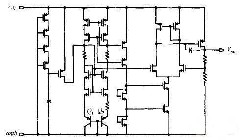
Figure 4 Circuit diagram of voltage regulator
2.2 Matching network and backscatter circuit
Unlike the 13.56MHz HF transponder, the UHF band RFID transponder uses a dipole antenna. Figure 5 is a SPICE (simulaTIon program with integrated circuit emphasis) equivalent circuit diagram of the transponder and the antenna. In this equivalent SPICE circuit model, the received RF carrier signal is Vs, the impedance of the antenna is Zs=Rs+jXL, which can be regarded as the internal resistance of the voltage source Vs, and the equivalent input impedance of the transponder chip is ZL= RL-jXL. Therefore, when ZL=Zs*, the impedance is matched and the power transmission is maximum. In the case of impedance matching, from the perspective of the transponder with antenna, the impedance obtained should be Z=2RL, so we get the relationship between the receiving power Pre and the voltage swing VS as side:

Then the voltage swing Vin input to both ends of the chip is:
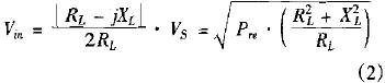
In order to achieve impedance matching, the circuit also needs to perform impedance transformation on the matching network, so that the internal resistance of the antenna and the input impedance of the radio frequency circuit part can achieve conjugate matching, so we use an L-type matching network. Due to the high cost of chip integrated inductors and low accuracy, we use the inductance of the antenna as a matching inductor to integrate the matching capacitor into the chip. After calculation, the input impedance of the radio frequency circuit is about (105-j406)Ω.
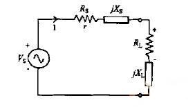
Figure 5 SPICE equivalent circuit diagram of transponder and antenna
Figure 6 is a schematic diagram of the backscatter circuit. The backscatter circuit uses a variable capacitor to change the impedance of the radio frequency circuit, thereby sending the transponder data to the RFID interrogator or card reader. The variable capacitance is realized by MOS varactor. In standard CMOS process, we can use the voltage-controlled variable capacitance from the gate of the MOS tube to the substrate, and use the gate of the MOS varactor as one end of the capacitor and the source end Connect with the drain terminal as the other end of the capacitor.
2.3 AM demodulator circuit
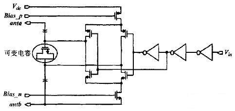
The AM demodulator circuit is used to restore the received modulated carrier into a digital signal for baseband processing. The demodulation circuit is composed of an envelope detection circuit, a filter circuit and a comparator (as shown in Figure 7). The comparator uses Hysteresis comparator to reduce the bit error rate. The envelope detector uses the same circuit as the rectifier to extract the envelope signal. The low-pass filter is used to eliminate noise signals and ripples on the power supply. Finally, the envelope signal is restored to a digital signal at the output of the comparator through the hysteresis comparator.
Figure 7 AM demodulator schematic diagram
2.4 Power-on reset circuit
The power-on reset circuit has two main functions. One is when the transponder enters the effective area of the interrogator or card reader and the power supply voltage has reached the normal working potential, it will generate a reset signal for the entire chip; the second is when the power supply voltage drops suddenly. When the circuit is reset, it can prevent the logic circuit from malfunctioning. Figure 8 is a power-on reset circuit diagram, the power-on reset delay time of the circuit is 10μs. When the time continues to increase from zero and exceeds the pull-up voltage 2.4V, the P tube MP1 and the N tube MN1 are turned on first, making the potentials of points A and B gradually rise from 0 with the increase of Yu, after reverse phase The gate voltages of the MP2 and MN2 transistors all change linearly with the rise of VDD, so at the beginning, MN2 is turned on and MP2 is turned off, so that the voltage at point C is always 0 (effective reset). When VDD reaches a higher potential, the potential at point A also rises to a certain level at the same time, making the MN2 tube cut off. At this time, the MP2 tube is turned on and the potential at point C rises rapidly. After several levels of buffers, a slave is obtained. Logic 0 to 1 transition signal output, so that the circuit starts to work normally. The cascading of the following stages of buffers and capacitive loads is to obtain a time delay of about 10μs, that is, when VDD is higher than 2.4V and keeps 10μs, the reset signal completes the jump, so as to realize the stable operation of the circuit. The simulation results are as follows Shown in Figure 9.
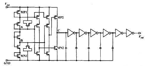
Figure 8 Power-on reset circuit schematic diagram
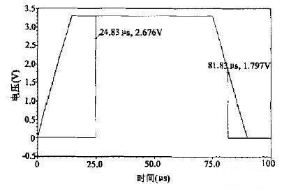
Figure 9 Power-on reset circuit simulation results
2.5 Local oscillator and clock generation circuit
Unlike the 13.56MHz HF transponder, the 915MHz UHF transponder cannot obtain a local clock from the carrier frequency, but can only provide a clock for the digital logic circuit part through a built-in low-power local oscillator. The clock frequency can accept an error of ±30%, and the accuracy of the clock frequency is not high, so a relatively simple oscillator structure can be used to reduce the power consumption of the chip. After analysis, we decided to use a ring oscillator composed of odd-numbered fully differential inverters, which not only can well suppress the change of common-mode voltage, but also can obtain good power supply suppression characteristics. Figure 10 is a schematic diagram of the local oscillator and clock generation circuit. After simulation test, considering the full conditions of temperature, power supply voltage and process angle changes, the output frequency of the circuit is about 250kHz, and its variation error ensures that the bit rate accuracy of the data is less than 15% of VDD. The performance has no impact, and the system design requirements are better met. Figure 11 shows the clock signal obtained by simulation.
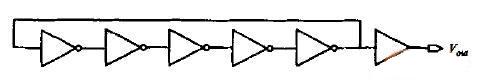
Figure 10 Schematic diagram of local oscillator and clock generation circuit
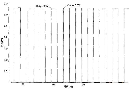
Figure 11 Clock signal obtained by simulation
3 Test results and analysis
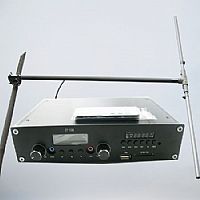
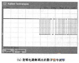
The radio frequency circuit chip adopts Chartered 0.35μm 2P4M CMOS process which supports Schottky diode and EEPROM for tapeout. The core circuit chip area without I/O pads (PAD) is 300μm×720μm. Except for the two PADs used to connect to external antennas, the remaining PADs are used for chip function testing. Figure 12 is the waveform diagram obtained after the radio frequency circuit chip is connected to the external antenna and the card reader is tested for communication. The test is carried out using the THM6BC1-915 UHF RFID card reader of Beijing Tsinghua Tongfang Microelectronics Co., Ltd. that meets the ISO/IEC 18000-6B standard . Figure 12(a) is the VDD waveform obtained by the rectifier and voltage regulator circuit after receiving the radio frequency signal transmitted by the card reader. The average value is 3.3V, and there is only a ripple less than 20mV, which is well satisfied The design index requirements are met. Figure 12(b) shows the digital signal sent by the card reader obtained by the RF circuit chip demodulation. After testing, when the EIRP is 4W (36dBm) and the antenna gain is OdB, the radio frequency circuit chip works at 915MHz, the reading distance is greater than 3m, and the working current is less than 8μA.
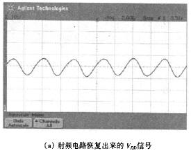
Figure 12 Test waveform diagram of RF circuit chip
4 Conclusion
This paper proposes a high-performance and low-power passive UHF RFID transponder chip radio frequency circuit that meets the ISO/IEC 18000-6B standard. The radio frequency circuit works at 915MHz and has no external components other than the antenna. It uses Schottky diodes. The rectifier receives energy from the radio frequency electromagnetic field. The chartered 0.35μm 2P4M CMQS process which supports Schottky diodes and EEPROM is used for tapeout, and its core area is 300μm×720μm. The RFID radio frequency circuit includes several main modules such as local oscillator, clock generation circuit, reset circuit, matching network and backscatter circuit, rectifier, voltage regulator and AM demodulator. This text designs and optimizes each module circuit, designs the low power consumption radio frequency circuit that accords with the standard requirement. The test was carried out with a THM6BC1-915Y2 UHF RFID card reader that conforms to the ISO/IEC 18000-6B standard. The test results show that the reading distance is greater than 3m, and the result satisfies the index requirements of the passive UHF RFID transponder system.
Our other product: